Mar. 2002
MITSUBISHI GATE COMMUTATED TURN-OFF THYRISTOR UNIT
GCU35AB-120
HIGH POWER INVERTER USE
PRESS PACK TYPE
GCU35AB-120
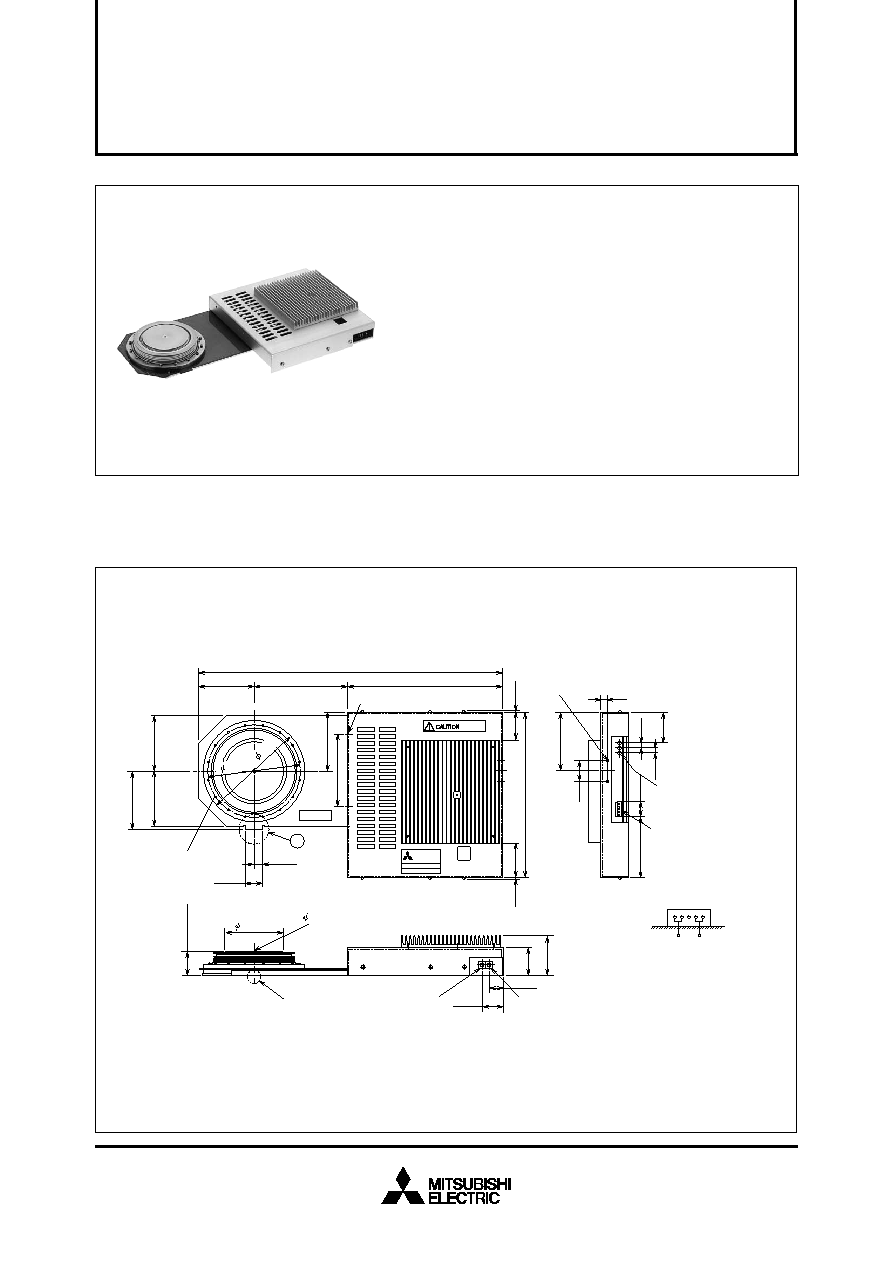
OUTLINE DRAWING
Dimensions in mm
APPLICATION
Inverters, DC choppers, Induction heaters, DC to DC converters.
PRELIMINARY
Notice: This is not a final specification.
Some parametric limits are subject to change.
(447)
16-M3
◊
0.5
2-M2
◊
0.7
(137)
(80)
(230)
(40.5)
(35.5)
Fault signal output
(HFBR-1528)
Fiber optics input
(HFBR-2528)
Fiber optics enter
(25.5)
58
±
1
Explanation of
terminal numbers
~
~
26V
±
2V
(AC rectangular)
1
5
(85)
(105)
(80)
(81.13)
(85.72)
Status LED's
Green ,power supply
Yellow ,GCT on command
Red ,GK short
Connector for
power supply
B5PS-VH(JST)
(10)
(7.5)
(40)
(2.5)
(240)
(44)
(7.5)
(19.7)
(88)
(50)
(2.5)
(85)
(30)
2-M4
◊
0.7
(12.7)
C
B
(25.4)
85
±
0.2
3.5
±
0.2 2.2
±
0.2 DEPTH
34.5
±
0.5
TYPE
GATE DRIVER
GCT THYRISTPR
HIGT VOLTAGE
BU-E40
SERIAL
00000000-00
(
134)
(
148)
q
Asymmetrical GCT unit
q
GCT and Gate driver are connected
q
I
TQRM
Repetitive controllable
on-state current .................................. 3500A
q
I
T(AV)
Average on-state current .................... 1200A
q
V
DRM
Repetitive peak off-state voltage .................. 6000V
q
V
RRM
Repetitive peak reverse voltage ....................... 21V
Mar. 2002
On-state voltage
Repetitive peak reverse current
Repetitive peak off-state current
Reverse gate current
Gate trigger current
Gate trigger voltage
Thermal resistance
--
--
--
--
--
--
--
--
3.8
100
150
100
2.5
1.5
0.011
--
--
--
--
--
--
--
I
T
= 3500A, T
j
= 125
∞
C
V
RM
= 21V, T
j
= 125
∞
C
V
DM
= 6000V, V
GK
= ≠2V, T
j
= 125
∞
C
V
RG
= 21V, T
j
= 125
∞
C
V
D
= 3600V, V
GK
= ≠2V, T
j
= 125
∞
C
(Expo. wave)
V
D
= 3600V, I
T
= 3500A, d
i
/d
t
= 1000A/
µ
s, T
j
= 125
∞
C
With GU-E40
(see Fig. 1, 2)
V
DM
= 6000V, V
D
= 3600V, I
T
= 3500A
V
RG
= 20V, T
j
= 125
∞
C
With GU-E40
(see Fig. 1, 3)
Junction to Fin
V
TM
I
RRM
I
DRM
I
GRM
I
GT
V
GT
R
th(j-f)
E
on
t
s
Turn-off switching energy
t
gt
Turn-on switching energy
Unit
Symbol
V
RRM
V
RSM
V
DRM
V
DSM
V
LTDS
Parameter
V
V
V
V
V
Voltage class
21
21
6000
6000
3600
Repetitive peak reverse voltage
Non-repetitive peak reverse voltage
Repetitive peak off-state voltage
Non-repetitive peak off-state voltage
Long term DC stability voltage
MAXIMUM RATINGS
MITSUBISHI GATE COMMUTATED TURN-OFF THYRISTOR UNIT
GCU35AB-120
HIGH POWER INVERTER USE
PRESS PACK TYPE
GCT PART (Type name : FGC3500AX-120DS)
Conditions
--
--
V
GK
= ≠2V
V
GK
= ≠2V
V
GK
= ≠2V,
= 100 Fit
1800
1200
25
2.6
◊
10
6
10
21
1000
3500
10
120
200
630
≠20 ~ +125
≠20 ~ +150
32 ~ 48
1500
V
DM
= 6000V, V
D
= 3600V, V
RG
= 20V, L
C
= 0.3
µ
H
T
j
= 25/125
∞
C, With GU-E40
(see Fig. 1, 3)
Applied for all condition angles
f = 60Hz, sinewave
= 180
∞
, T
f
= 70
∞
C
V
D
= 3600V, I
T
= 3500A, T
j
= 25/125
∞
C, f = 60Hz
With GU-E40
(see Fig. 1,2 )
(Recommended value 40kN)
Typical value
One half cycle at 60Hz, T
j
= 125
∞
C Start
Ratings
A
A
kA
A
2
s
V
V
A
A
kW
kW
W
W
∞
C
∞
C
kN
g
RMS on-state current
Average on-state current
Surge on-state current
Current-squared, time integration
Peak forward gate voltage
Peak reverse gate voltage
Peak forward gate current
Peak reverse gate current
Peak forward gate power dissipation
Peak reverse gate power dissipation
Average forward gate power dissipation
Average reverse gate power dissipation
Operation junction temperature
Storage temperature
Mounting force required
Weight
I
T(RMS)
I
T(AV)
I
TSM
I
2t
V
FGM
V
RGM
I
FGM
I
RGM
P
FGM
P
RGM
P
FG(AV)
P
RG(AV)
T
j
T
stg
--
--
Symbol
Parameter
Conditions
I
TQRM
Repetitive controllable on-state current
3500
Unit
A
d
iT
/d
t
Critical rate of rise of on-state current
1000
A/
µ
s
V
mA
mA
mA
A
V
K/W
ELECTRICAL CHARACTERISTICS
Symbol
Parameter
Conditions
Limits
Min
Typ
Max
Unit
V
D
= 24V, R
L
= 0.1
, T
j
= 25
∞
C
DC method
d
v
/d
t
Critical rate of rise of off-state voltage
Turn-on time
E
off
Storage time
3000
--
--
--
--
--
1.2
--
19
--
3.0
--
3.0
--
V/
µ
s
µ
s
J/P
µ
s
J/P
PRELIMINARY
Notice: This is not a final specification.
Some parametric limits are subject to change.
t
d
Turn-on delay time
--
--
1.0
µ
s

Mar. 2002
td ; 0V
RG
~ 0.9V
D
t
gt
; 0V
RG
~ 0.1V
D
t
s
; 0V
RG
~ 0.9I
T
di
G
/d
t
; 0.1I
GM
~ 0.9I
GM
tw
; 0V
RG
~ 0.9I
GM
di
GQ
/d
t
; 0.1I
RG
~ 0.9I
RG
t
fd
; 50%on signal ~ 0V
RG
t
rd
; 50%off signal ~ 0V
RG
V
D
V
RG
I
GM
ts
V
RG
I
T
V
D
di
GQ
/dt
di
G
/dt
I
GQ
I
G
DUT
L
V
D
Rc
L(load)
FWDi
DUT
CDi
Cc
V
D
Lc
ANL
tgt
td
t
fd
trd
Control signal
tw
MITSUBISHI GATE COMMUTATED TURN-OFF THYRISTOR UNIT
GCU35AB-120
HIGH POWER INVERTER USE
PRESS PACK TYPE
PRELIMINARY
Notice: This is not a final specification.
Some parametric limits are subject to change.
Fig. 1 Turn-on and Turn-off waveform
Fig. 2 Turn-on test circuit
Fig. 3 Turn-off test circuit
(With clamp circuit)
Power supply voltage (Note 1)
Power supply current (Note 1)
Control signal
Frequency
Delay time of on gate current
Delay time of off gate current
Critical rate of rise of on gate current
Peak on gate current
Width of on high gate current
On gate current
Critical rate of rise of off gate current
Maximum duty
Temperature
Weight
Thermal resistance
(Junction to Fin)
(Note 2)
Status signal
(Note 3)
AC rectangular, f = 15kHz ~ 100kHz or DC power supply
I
T
= 1500Arms, f = 500Hz, duty = 0.5
Optical fiber data link
Transmitter : HFBR-1528 (HP)
Receiver : HFBR-2528 (HP)
I
T
= 1500Arms, duty = 0.5
Ta = 25
∞
C
Ta = 25
∞
C
Tj
≠10
∞
C
V
RG
= 20V
Operation temperature (Recommend :
40
∞
C)
With FGC3500AX-120DS
With FGC3500AX-120DS
V
C
I
C
--
f
t
fd
t
rd
d
iG
/d
t
I
GM
t
W
I
G
d
iGQ
/d
t
D
max
Ta
--
Rth(j-f)
--
25.2
--
--
--
--
--
100
--
5
10
--
--
≠10
--
--
--
V
A
--
Hz
µ
s
µ
s
A/
µ
s
A
µ
s
A
A/
µ
s
%
∞
C
g
K/W
GATE DRIVER PART (Type name : GU-E40)
Symbol
Parameter
Conditions
Limits
Min
Typ
Max
Unit
28
--
--
--
--
--
--
200
--
--
6000
--
--
5300
--
--
32.2
5
--
500
2.0
2.0
--
--
--
--
--
100
+60
--
0.012
--
--

Mar. 2002
MITSUBISHI GATE COMMUTATED TURN-OFF THYRISTOR UNIT
GCU35AB-120
HIGH POWER INVERTER USE
PRESS PACK TYPE
PRELIMINARY
Notice: This is not a final specification.
Some parametric limits are subject to change.
Note 1. Main current condition of GCT Thyristor is 1500Arms, duty = 0.5, f = 500Hz.
2. If GU-E40 and FGC3500AX-120DS are used together, Rth(j-f) becomes 0.012K/W.
(Only FGC3500AX-120DS is used, Rth(j-f) becomes 0.011K/W)
3. Status signal from gate driver
(1) Status signal of LED
Green : Power supply
Yellow : GCT on command
Red
: GK short
(2) status signal of Optic Transmitter
Status signal
Control signal
Normal operation
No light
Light
Failure mode; Gate cathode short
Failure mode; Continuously turned off
Lower driver voltage
(for on or off gate power supply value)
Status signal
Control signal

Mar. 2002
PERFORMANCE CURVES
MITSUBISHI GATE COMMUTATED TURN-OFF THYRISTOR UNIT
GCU35AB-120
HIGH POWER INVERTER USE
PRESS PACK TYPE
PRELIMINARY
Notice: This is not a final specification.
Some parametric limits are subject to change.
0
0.004
0.006
0.002
0.01
0.012
0.008
0.014
5
3
10
1
0
1
2
3
4
5
6
7
2
7
5
3
2
7
5
3
2
7
0
0
25
20
15
10
5
500 1000 1500 2000 2500 3000 3500 4000
2.0
0
1.8
1.6
1.4
1.2
1.0
0.8
0.6
0.4
0.2
0
4000
3500
3000
2500
2000
1500
1000
500
10
4
10
2
10
3
Tj=125
∞
C
Tj=25
∞
C
MAXIMUM ON-STATE CHARACTERISTIC
ON-STATE CURRENT I
T
(
A
)
ON-STATE VOLTAGE V
TM
(V)
TURN ON SWITCHING ENERGY Eon (J/P)
TURN ON CURRENT I
T
(A)
Eon VS I
T
(TYPICAL)
TURN OFF SWITCHING ENERGY Eoff (J/P)
TURN OFF CURRENT I
T
(A)
Eoff VS I
T
(TYPICAL)
MAXIMUM THERMAL IMPEDANCE
CHARACTERISTIC
(JUNCTION TO FIN)
THERMAL IMPEDANCE Zth (K/W)
TIME (S)
Condition
V
D
=3600V, di/dt=1000A/
µ
s
Tj=125
∞
C
Condition
V
DM
=3600V+0.44
◊
I
T
V
D
=3600V, C
C
=6
µ
F
L
C
=0.3
µ
H, Tj=125
∞
C
10
≠2
10
≠1
2 3 5 7
10
0
2 3 5 7
10
1
2 3 5 7
10
≠3
2 3 5 7