 | –≠–ª–µ–∫—Ç—Ä–æ–Ω–Ω—ã–π –∫–æ–º–ø–æ–Ω–µ–Ω—Ç: M54531FP | –°–∫–∞—á–∞—Ç—å:  PDF PDF  ZIP ZIP |

Aug. 1999
PIN CONFIGURATION
MITSUBISHI SEMICONDUCTOR <TRANSISTOR ARRAY>
M54531P/FP
7-UNIT 400mA DARLINGTON TRANSISTOR ARRAY WITH CLAMP DIODE
DESCRIPTION
M54531P and M54531FP are seven-circuit Darlington tran-
sistor arrays with clamping diodes. The circuits are made of
NPN transistors. Both the semiconductor integrated circuits
perform high-current driving with extremely low input-current
supply.
FEATURES
High breakdown voltage (BV
CEO
40V)
High-current driving (Ic(max) = 400mA)
With clamping diodes
Driving available with PMOS IC output
Wide input voltage range (V
I
= ≠40 to +40V)
Wide operating temperature range (Ta = ≠20 to +75
∞
C)
APPLICATION
Drives of relays and printers, digit drives of indication ele-
ments (LEDs and lamps), and MOS-bipolar logic IC inter-
faces
FUNCTION
The M54531P and M54531FP each have seven circuits con-
sisting of NPN Darlington transistors. A serial circuit includ-
ing a diode and resistance of 20k
is provided between in-
put transistor bases and input pins. A spike-killer clamping
diode is provided between each output pin (collector) and
COM pin (pin 9). The output transistor emitters are all con-
nected to the GND pin (pin 8).
The collector current is 400mA maximum. Collector-emitter
supply voltage is 40V maximum.
The M54531FP is enclosed in a molded small flat package,
enabling space-saving design.
CIRCUIT DIAGRAM
V
mA
V
mA
V
W
∞
C
∞
C
≠0.5 ~ +40
400
≠40 ~ +40
400
40
1.47(P)/1.00(FP)
≠20 ~ +75
≠55 ~ +125
V
CEO
I
C
V
I
I
F
V
R
P
d
T
opr
T
stg
20K
2K
20K
COM
GND
INPUT
OUTPUT
The diode, indicated with the dotted line, is parasitic, and cannot
be used.
Unit :
The seven circuits share the COM and GND.
Ratings
Symbol
Parameter
Conditions
Unit
ABSOLUTE MAXIMUM RATINGS
(Unless otherwise noted, Ta = ≠20 ~ +75
∞
C)
Collector-emitter voltage
Collector current
Input voltage
Clamping diode forward current
Clamping diode reverse voltage
Power dissipation
Operating temperature
Storage temperature
Output, H
Current per circuit output, L
Ta = 25
∞
C, when mounted on board
1
IN1
IN2
IN3
IN4
IN5
IN6
IN7
COM COMMON
GND
2
3
4
5
6
7
8
16
15
14
13
12
11
10
9
O7
O6
O5
O4
O3
O2
O1
16P4(P)
Package type 16P2N-A(FP)
INPUT
OUTPUT
POWEREX

Aug. 1999
MITSUBISHI SEMICONDUCTOR <TRANSISTOR ARRAY>
M54531P/FP
7-UNIT 400mA DARLINGTON TRANSISTOR ARRAY WITH CLAMP DIODE
RECOMMENDED OPERATING CONDITIONS
(Unless otherwise noted, Ta = ≠20 ~ +75
∞
C)
V
µ
A
V
µ
A
--
V
V
V
O
V
IL
--
--
--
--
0
9
6
0
40
1
I
C
V
IH
0
0
--
--
400
200
35
mA
V
I
I
V
CE (sat)
40
--
--
--
--
--
--
--
1000
--
1.3
1.0
1.1
2.0
--
1.4
--
3500
--
2.4
1.6
1.8
3.8
≠20
2.4
100
--
V
mA
+
: The typical values are those measured under ambient temperature (Ta) of 25
∞
C. There is no guarantee that these values are obtained under any
conditions.
ns
ns
--
--
30
680
--
--
TIMING DIAGRAM
NOTE 1 TEST CIRCUIT
PG
50
C
L
Measured device
OPEN
V
O
R
L
INPUT
OUTPUT
(1) Pulse generator (PG) characteristics : PRR = 1kHz,
tw = 10
µ
s, tr = 6ns, tf = 6ns, Z
O
= 50
V
P
= 9V
P-P
(2) Input-output conditions : R
L
= 25
, V
O
= 10V
(3) Electrostatic capacity C
L
includes floating capacitance at
connections and input capacitance at probes
Parameter
Limits
min
typ
max
Symbol
Unit
Output voltage
Collector current
(Current per 1 cir-
cuit when 7 circuits
are coming on si-
multaneously)
Duty Cycle
P : no more than 8%
FP : no more than 6%
Duty Cycle
P : no more than 30%
FP : no more than 25%
"L" input voltage
"H" input voltage
I
C
400mA
I
C
200mA
I
CEO
= 100
µ
A
V
I
= 9V, I
C
= 400mA
V
I
= 6V, I
C
= 200mA
V
I
= 18V
V
I
= 35V
V
I
= ≠35V
I
F
= 400mA
V
R
= 40V
V
CE
= 4V, I
C
= 300mA, Ta = 25
∞
C
Collector-emitter breakdown voltage
Input reverse current
Clamping diode forward voltage
Clamping diode reverse current
DC amplification factor
Symbol
Unit
Parameter
Test conditions
Limits
min
typ
+
max
Collector-emitter saturation voltage
Input current
ELECTRICAL CHARACTERISTICS
(Unless otherwise noted, Ta = ≠20 ~ +75
∞
C)
V
(BR) CEO
I
IR
V
F
I
R
h
FE
Symbol
Unit
Parameter
Test conditions
Limits
min
typ
max
SWITCHING CHARACTERISTICS
(Unless otherwise noted, Ta = 25
∞
C)
Turn-on time
Turn-off time
C
L
= 15pF (note 1)
t
on
t
off
ton
50%
50%
50%
50%
toff
INPUT
OUTPUT
POWEREX

Aug. 1999
MITSUBISHI SEMICONDUCTOR <TRANSISTOR ARRAY>
M54531P/FP
7-UNIT 400mA DARLINGTON TRANSISTOR ARRAY WITH CLAMP DIODE
TYPICAL CHARACTERISTICS
Thermal Derating Factor Characteristics
Ambient temperature Ta (∞C)
M54531FP
M54531P
Power dissipation Pd (W)
0
0
0.5
1.0
1.5
2.0
25
50
75
100
Output Saturation Voltage
Collector Current Characteristics
Output saturation voltage V
CE
(sat) (V)
0
0
100
200
V
I
= 6V
Ta = ≠20∞C
Ta = 25∞C
Ta = 75∞C
300
400
0.4
0.8
1.2
1.6
Collector current Ic (mA)
Duty-Cycle-Collector Characteristics
(M54531P)
Duty cycle (%)
∑The collector current values
represent the current per circuit.
∑Repeated frequency
10Hz
∑The value in the circle represents the
value of the simultaneously-operated circuit.
∑Ta = 25∞C
∑The collector current values
represent the current per circuit.
∑Repeated frequency
10Hz
∑The value in the circle represents the
value of the simultaneously-operated circuit.
∑Ta = 25∞C
0
0
100
200
300
400
500
20
40
60
80
100
Collector current Ic (mA)
∑The collector current values
represent the current per circuit.
∑Repeated frequency
10Hz
∑The value in the circle represents the
value of the simultaneously-operated circuit.
∑Ta = 75∞C
∑The collector current values
represent the current per circuit.
∑Repeated frequency
10Hz
∑The value in the circle represents the
value of the simultaneously-operated circuit. ∑Ta = 75∞C
Duty-Cycle-Collector Characteristics
(M54531P)
Duty cycle (%)
0
0
100
200
300
400
500
20
40
60
80
100
Collector current Ic (mA)
Duty-Cycle-Collector Characteristics
(M54531FP)
Duty cycle (%)
0
0
100
200
300
400
500
20
40
60
80
100
Collector current Ic (mA)
Duty-Cycle-Collector Characteristics
(M54531FP)
Duty cycle (%)
0
0
100
200
300
400
500
20
40
60
80
100
Collector current Ic (mA)
POWEREX
Aug. 1999
MITSUBISHI SEMICONDUCTOR <TRANSISTOR ARRAY>
M54531P/FP
7-UNIT 400mA DARLINGTON TRANSISTOR ARRAY WITH CLAMP DIODE
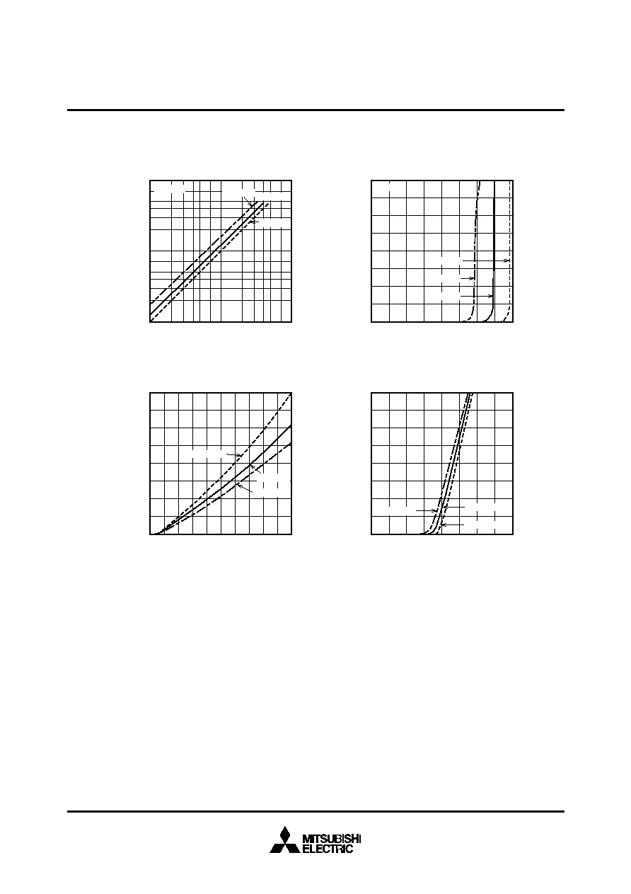
DC Amplification Factor
Collector Current Characteristics
Collector current Ic (mA)
10
1
10
3
V
CE
= 4V
Ta = 25∞C
Ta = 75∞C
Ta = ≠20∞C
5
3
2
7
10
4
5
3
2
7
10
3
10
2
2
3
5
7
10
2
2
3
5
7
DC amplification factor h
FE
Grounded Emitter Transfer Characteristics
Input voltage V
I
(V)
0
V
CE
= 4V
Ta = 75∞C
Ta = ≠20∞C
Ta = 25∞C
100
200
300
400
0
1
2
3
4
Collector current Ic (mA)
Input Characteristics
Input voltage V
I
(V)
0
Ta = 25∞C
Ta = 75∞C
Ta = ≠20∞C
0.5
1.0
1.5
2.0
0
5
10
15
20
25
Input current I
I
(mA)
Clamping Diode Characteristics
Forward bias voltage V
F
(V)
0
0
100
200
Ta = ≠20∞C
Ta = 25∞C
Ta = 75∞C
300
400
0.5
1.0
1.5
2.0
Forward bias current I
F
(mA)
POWEREX