 | –≠–ª–µ–∫—Ç—Ä–æ–Ω–Ω—ã–π –∫–æ–º–ø–æ–Ω–µ–Ω—Ç: M54583FP | –°–∫–∞—á–∞—Ç—å:  PDF PDF  ZIP ZIP |

Aug.1999
PIN CONFIGURATION (TOP VIEW)
MITSUBISHI SEMICONDUCTOR <TRANSISTOR ARRAY>
M54583P/FP
8-UNIT 400mA DARLINGTON TRANSISTOR ARRAY
DESCRIPTION
M54583P and M54583FP are eight-circuit collector-current-
synchronized Darlington transistor arrays. The circuits are
made of PNP and NPN transistors. Both the semiconductor
integrated circuits perform high-current driving with ex-
tremely low input-current supply.
FEATURES
q
High breakdown voltage (BV
CEO
50V)
q
High-current driving (Ic(max) = 400mA)
q
Active L-level input
q
With input clamping diodes
q
Wide operating temperature range (Ta = ≠20 to +75
∞
C)
APPLICATION
Interfaces between microcomputers and high-voltage, high-
current drive systems, drives of relays and printers, and
MOS-bipolar logic IC interfaces
FUNCTION
The M54583 is produced by adding PNP transistors to
M54523 inputs. Eight circuits having active L-level inputs are
provided.
Resistance of 7k
and diode are provided in series between
each input and PNP transistor base. The input diode is in-
tended to prevent the flow of current from the input to the
V
CC
. Without this diode, the current flow from "H" input to the
V
CC
and the "L" input circuits is activated, in such case where
one of the inputs of the 8 circuits is "H" and the others are "L"
to save power consumption. The diode is inserted to prevent
such misoperation.
This device is most suitable for a driver using NMOS IC out-
put especially for the driver of current sink.
Collector current is 400mA maximum. Collector-emitter sup-
ply voltage is 50V.
The 54583FP is enclosed in a molded small flat package,
enabling space saving design.
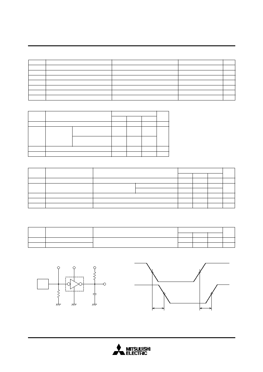
CIRCUIT DIAGRAM (EACH CIRCUIT)
1
IN1
INPUT
OUTPUT
IN2
IN3
IN4
IN5
IN6
IN7
V
CC
V
CC
O8
IN8
GND
2
3
4
5
6
7
8
9
18
17
16
15
14
13
12
11
10
O7
O6
O5
O4
O3
O2
O1
Outline 18P4G
M54583P
M54583FP
1
NC
INPUT
OUTPUT
NC : No connection
IN1
IN2
IN3
IN4
IN5
IN6
O8
IN7
IN8
2
3
4
5
6
7
8
9
20
19
18
17
16
15
14
13
12
GND
10
11
O7
O6
O5
O4
O2
O3
O1
NC
Outline 20P2N-A
7k
2.7k
7k
7.2k
3k
INPUT
GND
V
CC
OUTPUT
The eight circuits share the V
CC
and GND.
The diode, indicated with the dotted line, is parasitic, and cannot
be used.
Unit :
POWEREX
Aug.1999
ton
50%
50%
50%
50%
toff
INPUT
OUTPUT
PG
50
C
L
R
L
V
CC
V
O
INPUT
OUTPUT
(1) Pulse generator (PG) characteristics : PRR = 1kHz,
tw = 10
µ
s, tr = 6ns, tf = 6ns, Z
O
= 50
V
I
= 0.4 to 4V
(2) Input-output conditions : R
L
= 30
, V
O
= 10V, V
CC
= 4V
(3) Electrostatic capacity C
L
includes floating capacitance at
connections and input capacitance at probes
Measured
device
MITSUBISHI SEMICONDUCTOR <TRANSISTOR ARRAY>
M54583P/FP
8-UNIT 400mA DARLINGTON TRANSISTOR ARRAY
TIMING DIAGRAM
NOTE 1 TEST CIRCUIT
10
≠0.5 ~ +50
≠0.5 ~ V
CC
400
1.79/1.1
≠20 ~ +75
≠55 ~ +125
V
V
V
mA
W
∞
C
∞
C
ABSOLUTE MAXIMUM RATINGS
(Unless otherwise noted, Ta = ≠20 ~ +75
∞
C)
Ratings
Unit
Symbol
Parameter
Conditions
Supply voltage
Collector-emitter voltage
Input voltage
Collector current
Power dissipation
Operating temperature
Storage temperature
Output, H
Current per circuit output, L
Ta = 25
∞
C, when mounted on board
V
CC
V
CEO
V
I
I
C
P
d
T
opr
T
stg
ns
ns
t
on
t
off
--
--
130
3200
--
--
Symbol
Unit
Parameter
Test conditions
Limits
min
typ
max
SWITCHING CHARACTERISTICS
(Unless otherwise noted, Ta = 25
∞
C)
C
L
= 15pF (note 1)
Turn-on time
Turn-off time
V
V
V
8
V
CC
V
CC
≠3.6
5
--
--
4
V
CC
≠0.7
0
V
CC
V
IH
V
IL
Collector current
Per channel
RECOMMENDED OPERATING CONDITIONS
(Unless otherwise noted, Ta = ≠20 ~ +75
∞
C)
I
C
0
0
--
--
mA
350
200
Parameter
Limits
Symbol
Unit
Supply voltage
min
typ
max
"H" input voltage
"L" input voltage
V
CC
= 5V, Duty Cycle
P : no more than 34%
FP : no more than 15%
V
CC
= 5V, Duty Cycle
P : no more than 10%
FP : no more than 5%
V
µ
A
mA
--
V
(BR) CEO
I
I
I
CC
h
FE
V
V
CE (sat)
--
2.2
1.6
≠600
3
--
I
CEO
= 100
µ
A, V
CC
= 8V
V
I
= V
CC
≠3.6V
V
CC
= 5V, V
I
= V
CC
≠3.6V
V
CE
= 4V, V
CC
= 5V, I
C
= 350mA, Ta = 25
∞
C
Symbol
Unit
Parameter
Test conditions
Limits
min
typ
+
max
50
--
--
--
--
2000
--
1.1
0.98
≠320
--
10000
+
: The typical values are those measured under ambient temperature (Ta) of 25
∞
C. There is no guarantee that these values are obtained under any
conditions.
Collector-emitter breakdown voltage
Input current
Supply current (one circuit coming on)
DC amplification factor
Collector-emitter saturation voltage
ELECTRICAL CHARACTERISTICS
(Unless otherwise noted, Ta = ≠20 ~ +75
∞
C)
I
C
= 350mA
I
C
= 200mA
V
I
= V
CC
≠3.6V
POWEREX
Aug.1999
MITSUBISHI SEMICONDUCTOR <TRANSISTOR ARRAY>
M54583P/FP
8-UNIT 400mA DARLINGTON TRANSISTOR ARRAY
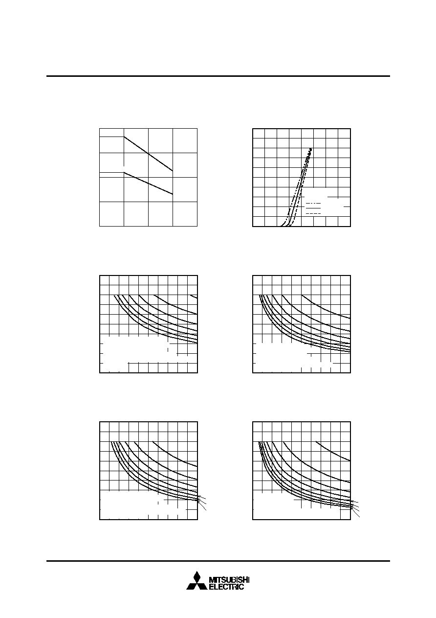
TYPICAL CHARACTERISTICS
Thermal Derating Factor Characteristics
Ambient temperature Ta (
∞
C)
Power dissipation Pd (W)
0
0
0.5
1.0
1.5
2.0
25
50
75
100
Output Saturation Voltage
Collector Current Characteristics
Output saturation voltage V
CE
(sat) (V)
Collector current Ic (mA)
Ta = ≠20
∞
C
Ta = 25
∞
C
Ta = 75
∞
C
V
I
= 1.4V
V
CC
= 5V
Ta = ≠20
∞
C
Ta = 25
∞
C
Ta = 75
∞
C
0
100
200
300
400
500
0
2.0
0.5
1.0
1.5
M54583P
M54583FP
Duty cycle (%)
1
2
3
4
Collector current Ic (mA)
Duty-Cycle-Collector Characteristics
(M54583P)
0
100
200
300
400
500
0
20
40
60
80
100
6
5
7
8
Duty cycle (%)
1
2
3
4
Collector current Ic (mA)
Duty-Cycle-Collector Characteristics
(M54583FP)
0
100
200
300
400
500
0
20
40
60
80
100
6
5
7
8
Duty cycle (%)
1
2
3
4
Collector current Ic (mA)
Duty-Cycle-Collector Characteristics
(M54583P)
0
100
200
300
400
500
0
20
40
60
80
100
6
5
7
8
∑The collector current values
represent the current per circuit.
∑Repeated frequency
10Hz
∑The value in the circle represents the
value of the simultaneously-operated circuit.
Duty cycle (%)
1
2
3
4
Collector current Ic (mA)
Duty-Cycle-Collector Characteristics
(M54583FP)
0
100
200
300
400
500
0
20
40
60
80
100
6
5
7
8
∑Vcc =5.0V
∑Ta = 75
∞
C
∑The collector current values
represent the current per circuit.
∑Repeated frequency
10Hz
∑The value in the circle represents the
value of the simultaneously-operated circuit.
∑V
CC
= 5V
∑Ta = 25
∞
C
∑The collector current values
represent the current per circuit.
∑Repeated frequency
10Hz
∑The value in the circle represents the
value of the simultaneously-operated circuit.
∑V
CC
= 5V ∑Ta = 75
∞
C
∑The collector current values
represent the current per circuit.
∑Repeated frequency
10Hz
∑The value in the circle represents the
value of the simultaneously-operated circuit.
∑V
CC
= 5V ∑Ta = 25
∞
C
POWEREX
Aug.1999
MITSUBISHI SEMICONDUCTOR <TRANSISTOR ARRAY>
M54583P/FP
8-UNIT 400mA DARLINGTON TRANSISTOR ARRAY
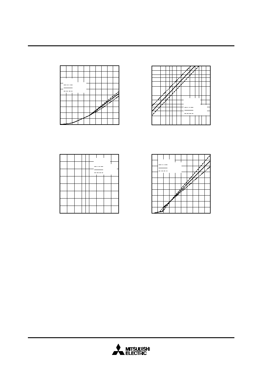
DC Amplification Factor
Collector Current Characteristics
Collector current Ic (mA)
DC amplification factor h
FE
10
1
10
2
3
2
2
5
7
10
3
3
5
7
10
2
10
3
3
5
7
10
4
3
2
2
5
7
Ta = ≠20
∞
C
Ta = 25
∞
C
Ta = 75
∞
C
V
CC
= 4V
V
CE
= 4V
Ta = ≠20
∞
C
Ta = 25
∞
C
Ta = 75
∞
C
Supply current Icc (mA)
0
100
200
300
400
0
Supply voltage V
CC
(V)
1.0
2.0
3.0
4.0
Supply Current Characteristics
Collector current Ic (mA)
Supply voltage-Input voltage V
CC≠
V
I
(V)
Grounded Emitter Transfer Characteristics
Ta = ≠20
∞
C
Ta = 25
∞
C
Ta = 75
∞
C
V
CC
= 4V
V
CE
= 4V
Ta = ≠20
∞
C
Ta = 25
∞
C
Ta = 75
∞
C
Ta = ≠20
∞
C
Ta = 25
∞
C
Ta = 75
∞
C
V
I
= 0V
Ta = ≠20
∞
C
Ta = 25
∞
C
Ta = 75
∞
C
0
1
2
3
4
5
0
2
4
6
8
10
Input Characteristics
Supply voltage-Input voltage V
CC≠
V
I
(V)
Input current I
I
(mA)
Ta = ≠20
∞
C
Ta = 25
∞
C
Ta = 75
∞
C
V
CC
= 5V
Ta = ≠20
∞
C
Ta = 25
∞
C
Ta = 75
∞
C
0
≠0.2
≠0.4
≠0.6
≠0.8
≠1.0
0
1
2
3
4
5
POWEREX