 | –≠–ª–µ–∫—Ç—Ä–æ–Ω–Ω—ã–π –∫–æ–º–ø–æ–Ω–µ–Ω—Ç: M63823P | –°–∫–∞—á–∞—Ç—å:  PDF PDF  ZIP ZIP |
Jan. 2000
Unit :
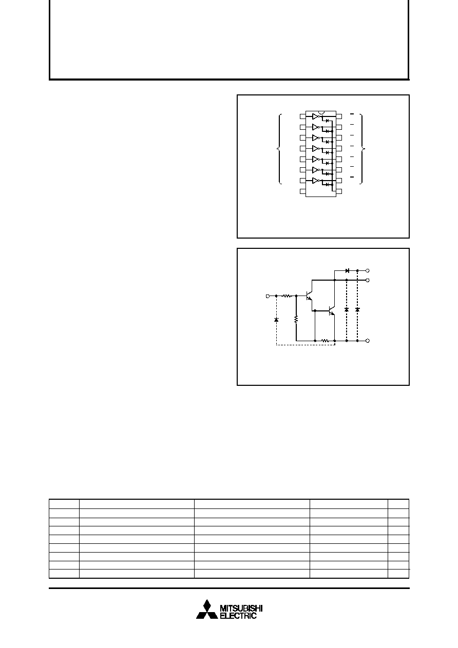
The seven circuits share the COM and GND
The diode, indicated with the dotted line, is parasitic, and
cannot be used.
INPUT
OUTPUT
GND
2.7k
3k
7.2k
COM
16P2N-A(FP)
IN7
O7
7
10
IN5
O5
5
12
INPUT
OUTPUT
IN4
O4
4
13
IN3
O3
3
14
IN2
O2
2
15
1
IN1
O1
16
GND
9
8
IN6
O6
6
11
16P4(P)
COM COMMON
16P2S-A(GP)
Package type
PIN CONFIGURATION
MITSUBISHI SEMICONDUCTOR <TRANSISTOR ARRAY>
M63823P/FP/GP
7-UNIT 500mA DARLINGTON TRANSISTOR-ARRAY WITH CLAMP DIODE
DESCRIPTION
M63823P, M63823FP and M63823GP are seven-circuit
Darlington transistor arrays with clamping diodes. The cir-
cuits are made of NPN transistors. Both the semi-conductor
integrated circuits perform high-current driving with ex-
tremely low input-current supply.
Production lineup has been newly expanded with the addi-
tion of 225mil (GP) package.
M63823P and M63823FP have the same pin connection as
M54523P and M54523FP. (Compatible with M54523P and
M54523FP) More over, the features of M63823P and
M63823FP are equal or superior to those of M54523P and
M54523FP.
FEATURES
q
Three package configurations (P, FP and GP)
q
Pin connection Compatible with M54523P and M54523FP
q
High breakdown voltage (BV
CEO
50V)
q
High-current driving (I
C(max)
= 500mA)
q
With clamping diodes
q
PMOS Compatible input
q
Wide operating temperature range (Ta = ≠40 to +85
∞
C)
APPLICATION
Drives of relays and printers, digit drives of indication ele-
ments (LEDs and lamps), and MOS-bipolar logic IC inter-
faces
FUNCTION
The M63823P, M63823FP and M63823GP each have seven
circuits consisting of NPN Darlington transistors. These ICs
have resistance of 2.7k
between input transistor bases and
input pins. A spike-killer clamping diode is provided between
each output pin (collector) and COM pin (pin 9). The output
transistor emitters are all connected to the GND pin (pin 8).
The collector current is 500mA maximum. Collector-emitter
supply voltage is 50V maximum.The M63823FP and
M63823GP is enclosed in molded small flat package, en-
abling space-saving design.
CIRCUIT DIAGRAM
Collector-emitter voltage
Collector current
Input voltage
Clamping diode forward current
Clamping diode reverse voltage
Power dissipation
Operating temperature
Storage temperature
V
mA
V
mA
V
W
∞
C
∞
C
≠0.5 ~ +50
500
≠0.5 ~ +30
500
50
1.47(P)/1.00(FP)/0.80(GP)
≠40 ~ +85
≠55 ~ +125
Ratings
Symbol
Parameter
Conditions
Unit
ABSOLUTE MAXIMUM RATINGS
(Unless otherwise noted, Ta = ≠40 ~ +85
∞
C)
Output, H
Current per circuit output, L
Ta = 25
∞
C, when mounted on board
V
CEO
I
C
V
I
I
F
V
R
P
d
T
opr
T
stg
POWEREX
Jan. 2000
ton
toff
50%
50%
50%
50%
INPUT
OUTPUT
(1)Pulse generator (PG) characteristics : PRR=1kHz,
tw = 10
µ
s, tr = 6ns, tf = 6ns, Zo = 50
V
P
= 3.85V
P-P
(2)Input-output conditions : R
L
= 25
, Vo = 10V
(3)Electrostatic capacity C
L
includes floating capacitance
at connections and input capacitance at probes
PG
50
R
L
OUTPUT
INPUT
Vo
C
L
OPEN
Measured device
--
--
--
I
C
400mA
I
C
200mA
Duty Cycle
P : no more than 8%
FP : no more than 5%
GP : no more than 4%
MITSUBISHI SEMICONDUCTOR <TRANSISTOR ARRAY>
M63823P/FP/GP
7-UNIT 500mA DARLINGTON TRANSISTOR-ARRAY WITH CLAMP DIODE
TIMING DIAGRAM
NOTE 1 TEST CIRCUIT
ns
ns
--
--
15
350
--
--
Symbol
Unit
Parameter
Test conditions
Limits
min
typ
max
Turn-on time
Turn-off time
t
on
t
off
C
L
= 15pF (note 1)
SWITCHING CHARACTERISTICS
(Unless otherwise noted, Ta = 25
∞
C)
RECOMMENDED OPERATING CONDITIONS
(Unless otherwise noted, Ta = ≠40 ~ +85
∞
C)
V
Parameter
0
Limits
min
typ
max
Symbol
Unit
V
O
Output voltage
"H" input voltage
"L" input voltage
Duty Cycle
P : no more than 30%
FP : no more than 20%
GP : no more than 15%
Collector current
(Current per 1 cir-
cuit when 7 circuits
are coming on si-
multaneously)
I
C
V
IL
V
IH
0
0
3.85
3.4
0
--
--
--
50
400
200
25
25
0.6
mA
V
V
--
1.2
1.0
0.9
0.9
1.4
--
2000
50
--
--
--
--
--
--
1000
V
(BR) CEO
I
I
V
F
I
R
h
FE
V
V
mA
V
µ
A
--
--
1.6
1.3
1.1
1.4
2.0
100
--
Symbol
Unit
Parameter
Test conditions
Limits
min
typ
max
Collector-emitter breakdown voltage
Input current
Clamping diode forward volltage
Clamping diode reverse current
DC amplification factor
I
CEO
= 100
µ
A
I
I
= 500
µ
A, I
C
= 350mA
I
I
= 350
µ
A, I
C
= 200mA
I
I
= 250
µ
A, I
C
= 100mA
V
I
= 3.85V
I
F
= 350mA
V
R
= 50V
V
CE
= 4V, I
C
= 350mA
V
CE(sat)
Collector-emitter saturation voltage
ELECTRICAL CHARACTERISTICS
(Unless otherwise noted, Ta = 25
∞
C)
POWEREX

Jan. 2000
MITSUBISHI SEMICONDUCTOR <TRANSISTOR ARRAY>
M63823P/FP/GP
7-UNIT 500mA DARLINGTON TRANSISTOR-ARRAY WITH CLAMP DIODE
TYPICAL CHARACTERISTICS
Thermal Derating Factor Characteristics
Ambient temperature Ta (
∞
C)
Power dissipation Pd(max) (W)
Output Saturation Voltage
Collector Current Characteristics
Output saturation voltage V
CE(sat)
(V)
Collector
current
Ic (mA)
Duty Cycle-Collector Characteristics
(M63823P)
Duty cycle (%)
Collector current Ic (mA)
Duty Cycle-Collector Characteristics
(M63823P)
Duty cycle (%)
Collector current Ic (mA)
Duty Cycle-Collector Characteristics
(M63823FP)
Duty cycle (%)
Collector current Ic (mA)
Duty Cycle-Collector Characteristics
(M63823FP)
Duty cycle (%)
Collector current Ic (mA)
2.0
1.5
1.0
0.5
0
0
25
50
75 85
100
M63823P
M63823FP
M63823GP
400
300
200
100
0
0
0.5
1.0
1.5
2.0
Ta = ≠40
∞
C
Ta = 25
∞
C
0.744
0.520
0.418
Ta = 85
∞
C
500
I
I
= 500
µ
A
500
400
300
200
100
0
0
100
20
40
60
80
1
2
3
4
5
6
7
∑The collector current values
represent the current per circuit.
∑Repeated frequencyy
10Hz
∑The value the circle represents the
value of the simultaneously-operated circuit.
∑Ta = 25
∞
C
500
400
300
200
100
0
0
100
20
40
60
80
1
2
3
4
5
6
7
∑The collector current values
represent the current per circuit.
∑Repeated frequency
10Hz
∑The value the circle represents the
value of the simultaneously-operated circuit.
∑Ta = 85
∞
C
500
400
300
200
100
0
0
100
20
40
60
80
1
2
3
4
5
6
7
∑The collector current values
represent the current per circuit.
∑Repeated frequency
10Hz
∑The value the circle represents the
value of the simultaneously-operated circuit.
∑Ta = 25
∞
C
500
400
300
200
100
0
0
100
20
40
60
80
1
2
3
4
5
6
7
∑The collector current values
represent the current per circuit.
∑Repeated frequency
10Hz
∑The value the circle represents the
value of the simultaneously-operated circuit. ∑Ta = 85
∞
C
POWEREX

Jan. 2000
MITSUBISHI SEMICONDUCTOR <TRANSISTOR ARRAY>
M63823P/FP/GP
7-UNIT 500mA DARLINGTON TRANSISTOR-ARRAY WITH CLAMP DIODE
Duty Cycle-Collector Characteristics
(M63823GP)
Duty cycle (%)
Collector current
Ic
(mA)
Duty Cycle-Collector Characteristics
(M63823GP)
Duty cycle (%)
Collector current
Ic
(mA)
Collector current Ic
C
(mA)
DC amplification f
actor
h
FE
Grounded Emitter Transfer Characteristics
DC Amplification Factor
Collector Current Characteristics
Input voltage V
I
(V)
Collector current Ic (mA)
Input Characteristics
Input voltage V
I
(V)
Input Current
I
I
(mA)
Clamping Diode Characteristics
Forward bias voltage V
F
(V)
F
orw
ard bias current I
F
(mA)
1
2
3
4
5
7
6
0
100
20
40
60
80
500
400
300
200
100
0
0
100
20
40
60
80
1
2
3
4
5
6
7
∑The collector current values
represent the current per circuit.
∑Repeated frequency
10Hz
∑The value the circle represents the
value of the simultaneously-operated circuit.
∑Ta = 25
∞
C
10
1
10
2
10
3
10
2
10
3
10
4
2
3
5 7
2
3
5 7
2
3
5
7
2
3
5
7
0
0
1
2
3
4
400
500
300
400
200
300
100
0
200
100
500
5
Ta = 25
∞
C
Ta = ≠40
∞
C
Ta = 85
∞
C
16
12
8
4
0
0
5
10
20
15
25
Ta = 85
∞
C
Ta = 25
∞
C
Ta = ≠40
∞
C
0
0.5
1.0
1.5
2.0
500
400
300
200
100
0
Ta = ≠40
∞
C
Ta = 25
∞
C
Ta = 85
∞
C
Ta = 85
∞
C
V
CE
= 4V
Ta = ≠40
∞
C
Ta= 25
∞
C
∑The collector current values
represent the current per circuit.
∑Repeated frequency
10Hz
∑The value the circle represents the
value of the simultaneously-operated circuit. ∑Ta = 85
∞
C
POWEREX