 | –≠–ª–µ–∫—Ç—Ä–æ–Ω–Ω—ã–π –∫–æ–º–ø–æ–Ω–µ–Ω—Ç: TOP234 | –°–∫–∞—á–∞—Ç—å:  PDF PDF  ZIP ZIP |

Æ
TOP232-234
TOPSwitch-FX
Family
Design Flexible,
EcoSmart
Æ
,
Integrated
Off-line Switcher
Figure 1. Typical Flyback Application.
Æ
PART
ORDER
NUMBER
3
Adapter
1
Open
Frame
2
Open
Frame
2
OUTPUT POWER TABLE
Table 1. Notes: 1. Typical continuous power in a non-ventilated
enclosed adapter measured at 50 ∞C ambient. 2. Maximum practical
continuous power in an open frame design with adequate heat sinking,
measured at 50 ∞C ambient. See key applications section for detailed
conditions. 3. Packages: P: DIP-8B, G: SMD-8B, Y: TO-220-7B.
PI-2503-073099
AC
IN
DC
OUT
D
S
C
TOPSwitch-FX
CONTROL
M
+
-
F
July 2001
Product Highlights
Lower System Cost, High Design Flexibility
∑ Features eliminate or reduce cost of external components
∑ Fully integrated soft-start for minimum stress/overshoot
∑ Externally settable accurate current limit
∑ Wider duty cycle for more power, smaller input capacitor
∑ Line under-voltage (UV) detection: no turn off glitches
∑ Line overvoltage (OV) shutdown extends line surge limit
∑ Line feed forward with maximum duty cycle (DC
MAX
)
reduction rejects ripple and limits DC
MAX
at high line
∑ Single resistor sets OV/UV thresholds, DC
MAX
reduction
∑ Frequency jittering reduces EMI and EMI filtering costs
∑ Regulates to zero load without dummy loading
∑ 132 kHz frequency reduces transformer/power supply size
∑ Half frequency option for video applications
∑ Hysteretic thermal shutdown for automatic recovery
∑ Large thermal hysteresis prevents PC board overheating
∑ Standard packages with omitted pins for large creepage
∑ Active-on and active-off remote ON/OFF capability
∑ Synchronizable to a lower frequency
EcoSmart
Æ
- Energy Efficient
∑ Cycle skipping reduces no-load consumption
∑ Reduced consumption in remote off mode
∑ Half frequency option for high efficiency standby
∑ Allows shutdown/wake-up via LAN/input port
Description
TOPSwitch-FX uses the proven TOPSwitch topology and cost
effectively integrates many new functions that reduce system
cost and, at the same time, improve design flexibility,
performance and energy efficiency. Like TOPSwitch, the high
voltage power MOSFET, PWM control, fault protection and
other control circuitry are all integrated onto a single CMOS
chip, but with two added terminals. The first one is a MULTI-
FUNCTION (M) pin, which implements programmable line
OV/UV shutdown and line feed forward/DC
MAX
reduction with
line voltage. The same pin can be used instead to externally set
an accurate current limit. In either case, this pin can also be used
for remote ON/OFF or to synchronize the oscillator to an
external, lower frequency signal. The second added terminal is
the FREQUENCY (F) pin and is available only in the Y
package. This pin provides the half frequency option when
connected to CONTROL (C) instead of SOURCE (S). The
features on the new pins can be disabled by shorting them to the
SOURCE, which allows the device to operate in a three terminal
TOPSwitch mode, but with the following new transparent
features: soft-start, cycle skipping, 132 kHz switching frequency,
frequency jittering, wider DC
MAX
, hysteretic thermal shutdown
and larger creepage. In addition, all critical parameters such as
frequency, current limit, PWM gain, etc. have tighter temperature
and absolute tolerances compared to the TOPSwitch-II family.
Higher current limit accuracy and larger DC
MAX
, when combined
with other features allow for a 10% to 15% higher power
capability on the TOPSwitch-FX devices compared to equivalent
TOPSwitch-II devices for the same input/output conditions.
TOP232P
TOP232G
TOP232Y
TOP233P
TOP233G
TOP233Y
TOP234P
TOP234G
TOP234Y
230 VAC
±
15%
Adapter
1
85-265 VAC
9 W
15 W
6.5 W
10 W
10 W
25 W
7 W
15 W
13 W
25 W
9 W
15 W
20 W
50 W
15 W
30 W
16 W
30 W
11 W
20 W
30 W
75 W
20 W
45 W

TOP232-234
2
B
7/01
Section List
Pin Functional Description ......................................................................................................................................... 3
TOPSwitch-FX Family Functional Description ......................................................................................................... 4
CONTROL (C) Pin Operation ................................................................................................................................. 4
Oscillator and Switching Frequency ....................................................................................................................... 5
Pulse Width Modulator and Maximum Duty Cycle ................................................................................................. 5
Minimum Duty Cycle and Cycle Skipping ............................................................................................................... 6
Error Amplifier ......................................................................................................................................................... 6
On-chip Current Limit with External Programability ................................................................................................ 6
Line Under-Voltage Detection (UV) ........................................................................................................................ 6
Line Overvoltage Shutdown (OV) ........................................................................................................................... 7
Line Feed Forward with DC
MAX
Reduction .............................................................................................................. 7
Remote ON/OFF and Synchronization ................................................................................................................... 7
Soft-Start ................................................................................................................................................................ 8
Shutdown/Auto-Restart .......................................................................................................................................... 8
Hysteretic Over-Temperature Protection ................................................................................................................ 8
Bandgap Reference ................................................................................................................................................ 8
High-Voltage Bias Current Source .......................................................................................................................... 8
Using FREQUENCY and MULTI-FUNCTION Pins ..................................................................................................... 9
FREQUENCY (F) Pin Operation ............................................................................................................................. 9
MULTI-FUNCTION (M) Pin Operation .................................................................................................................... 9
Typical Uses of FREQUENCY (F) Pin ...................................................................................................................... 11
Typical Uses of MULTI-FUNCTION (M) Pin ............................................................................................................. 12
Application Examples ............................................................................................................................................... 14
A High Efficiency, 30 W, Universal Input Power Supply ........................................................................................ 14
35 W Multiple Output Power Supply ..................................................................................................................... 15
17 W PC Standby Power Supply .......................................................................................................................... 16
Processor Controlled Supply Turn On/Off ............................................................................................................ 17
Key Application Considerations .............................................................................................................................. 19
TOPSwitch-FX vs. TOPSwitch-ll ........................................................................................................................... 19
TOPSwitch-FX Design Considerations ................................................................................................................. 20
TOPSwitch-FX Selection ................................................................................................................................ 20
Input Capacitor ............................................................................................................................................... 20
Primary Clamp and Output Reflected Voltage V
OR
......................................................................................... 20
Output Diode .................................................................................................................................................. 21
Soft-Start ........................................................................................................................................................ 21
EMI ................................................................................................................................................................. 21
Transformer Design ........................................................................................................................................ 21
Standby Consumption .................................................................................................................................... 23
TOPSwitch-FX Layout Considerations ................................................................................................................. 23
Primary Side Connections .............................................................................................................................. 23
Y-Capacitor..................................................................................................................................................... 23
Heat Sinking ................................................................................................................................................... 23
Quick Design Checklist ......................................................................................................................................... 23
Design Tools ......................................................................................................................................................... 23
Product Specifications and Test Conditions .......................................................................................................... 24
Typical Performance Characteristics ...................................................................................................................... 30
Package Outlines ...................................................................................................................................................... 34

TOP232-234
B
7/01
3
Figure 2. Functional Block Diagram.
Pin Functional Description
DRAIN (D) Pin:
High voltage power MOSFET drain output. The internal start-
up bias current is drawn from this pin through a switched high-
voltage current source. Internal current limit sense point for
drain current.
CONTROL (C) Pin:
Error amplifier and feedback current input pin for duty cycle
control. Internal shunt regulator connection to provide internal
bias current during normal operation. It is also used as the
connection point for the supply bypass and auto-restart/
compensation capacitor.
MULTI-FUNCTION (M) Pin:
Input pin for OV, UV, line feed forward with DC
MAX
reduction,
external set current limit, remote ON/OFF and synchronization.
A connection to SOURCE pin disables all functions on this pin
and makes TOPSwitch-FX operate in simple three terminal
mode (like TOPSwitch-II).
FREQUENCY (F) Pin: (Y package only)
Input pin for selecting switching frequency: 132 kHz if connected
to SOURCE pin and 66 kHz if connected to CONTROL pin.
Figure 3. Pin Configuration.
PI-2535-083099
The switching frequency is internally set for 132 kHz only
operation in P and G packages.
SOURCE (S) Pin:
Output MOSFET source connection for high voltage power
return. Primary side control circuit common and reference point.
SHUTDOWN/
AUTO-RESTART
PWM
COMPARATOR
CLOCK
SAW
HALF
FREQUENCY
OSCILLATOR WITH JITTER
CONTROLLED
TURN-ON
GATE DRIVER
CURRENT LIMIT
COMPARATOR
INTERNAL UV
COMPARATOR
INTERNAL
SUPPLY
5.8 V
4.8 V
SOURCE (S)
S
R
Q
Q
DMAX
STOP
SOFT-
START
-
+
CONTROL (C)
MULTI-
FUNCTION (M)
FREQUENCY (F)
(Y Package Only)
-
+
5.8 V
IFB
RE
ZC
VC
+
-
LEADING
EDGE
BLANKING
˜
8
1
HYSTERETIC
THERMAL
SHUTDOWN
SHUNT REGULATOR/
ERROR AMPLIFIER
+
-
DRAIN (D)
ON/OFF
DCMAX
VBG
DCMAX
VBG + VT
0
OV/UV
VI (LIMIT)
CURRENT
LIMIT
ADJUST
LINE
SENSE
SOFT START
PI-2501-031901
Tab Internally
Connected to SOURCE Pin
Y Package (TO-220-7B)
P Package (DIP-8B)
G Package (SMD-8B)
C
D
S
S
S
S
1 C
3 M
5 F
4 S
7 D
M
8
5
7
1
4
2
3
TOP232-234
4
B
7/01
TOPSwitch-FX
Family Functional Description
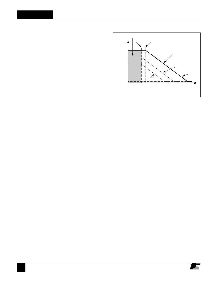
Figure 4. Relationship of Duty Cycle to CONTROL Pin Current.
PI-2504-072799
Duty Cycle (%)
I
C
(mA)
I
M
= 140
µ
A
I
M
= 190
µ
A
I
M
< I
M(DC)
1.9
1.5
5.5 5.9
Slope = PWM Gain
I
CD1
I
B
Auto-restart
78
1.5
47
Like TOPSwitch, TOPSwitch-FX is an integrated switched
mode power supply chip that converts a current at the control
input to a duty cycle at the open drain output of a high voltage
power MOSFET. During normal operation the duty cycle of the
power MOSFET decreases linearly with increasing CONTROL
pin current as shown in Figure 4.
In addition to the three terminal TOPSwitch features, such as the
high voltage start-up, the cycle-by-cycle current limiting, loop
compensation circuitry, auto-restart, thermal shutdown, etc.,
the TOPSwitch-FX incorporates many additional functions that
reduce system cost, increase power supply performance and
design flexibility. A patented high voltage CMOS technology
allows both the high voltage power MOSFET and all the low
voltage control circuitry to be cost effectively integrated onto a
single monolithic chip.
Two terminals, FREQUENCY (available only in Y package)
and MULTI-FUNCTION, have been added to implement some
of the new functions. These terminals can be connected to the
SOURCE pin to operate the TOPSwitch-FX in a TOPSwitch-
like three terminal mode. However, even in this three terminal
mode, the TOPSwitch-FX offers many new transparent features
that do not require any external components:
1. A fully integrated 10 ms soft-start reduces peak currents and
voltages during start-up and practically eliminates output
overshoot in most applications.
2. DC
MAX
of 78% allows smaller input storage capacitor, lower
input voltage requirement and/or higher power capability.
3. Cycle skipping at minimum pulse width achieves regulation
and very low power consumption at no load.
4. Higher switching frequency of 132 kHz reduces the
transformer size with no noticeable impact on EMI or on
high line efficiency.
5. Frequency jittering reduces EMI.
6. Hysteretic over-temperature shutdown ensures automatic
recovery from thermal fault. Large hysteresis prevents circuit
board overheating.
7. Packages with omitted pins and lead forming provide large
DRAIN creepage distance.
8. Tighter absolute tolerances and smaller temperature vari-
ations on switching frequency, current limit and PWM gain.
The MULTI-FUNCTION pin is usually used for line sensing by
connecting a resistor from this pin to the rectified DC high
voltage bus to implement line over-voltage (OV)/under-voltage
(UV) and line feed forward with DC
MAX
reduction. In this
mode, the value of the resistor determines the OV/UV thresholds
and the DC
MAX
is reduced linearly starting from a line voltage
above the under-voltage threshold. In high efficiency
applications, this pin can be used in the external current limit
mode instead, to reduce the current limit externally (to a value
close to the operating peak current), by connecting the pin to
SOURCE through a resistor. The same pin can also be used as
a remote ON/OFF and a synchronization input in both modes.
The FREQUENCY pin in the TO-220 package sets the switching
frequency to the default value of 132 kHz when connected to
SOURCE pin. A half frequency option can be chosen by
connecting this pin to CONTROL pin instead. Leaving this pin
open is not recommended.
CONTROL (C) Pin Operation
The CONTROL pin is a low impedance node that is capable of
receiving a combined supply and feedback current. During
normal operation, a shunt regulator is used to separate the
feedback signal from the supply current. CONTROL pin voltage
V
C
is the supply voltage for the control circuitry including the
MOSFET gate driver. An external bypass capacitor closely
connected between the CONTROL and SOURCE pins is
required to supply the instantaneous gate drive current. The
total amount of capacitance connected to this pin also sets the
auto-restart timing as well as control loop compensation.
When rectified DC high voltage is applied to the DRAIN pin
during start-up, the MOSFET is initially off, and the CONTROL
pin capacitor is charged through a switched high voltage current
source connected internally between the DRAIN and CONTROL
pins. When the CONTROL pin voltage V
C
reaches
approximately 5.8 V, the control circuitry is activated and the
soft-start begins. The soft-start circuit gradually increases the
duty cycle of the MOSFET from zero to the maximum value
over approximately 10 ms. If no external feedback/supply
current is fed into the CONTROL pin by the end of the soft-start,
the high voltage current source is turned off and the CONTROL
pin will start discharging in response to the supply current
drawn by the control circuitry. If the power supply is designed
properly, and no fault condition such as open loop or shorted
output exists, the feedback loop will close, providing external

TOP232-234
B
7/01
5
PI-2545-082299
S1
S2
S6
S7
S1
S2
S6
S7
S0
S1
S7
S0
S0
5.8 V
4.8 V
S7
0 V
0 V
0 V
V
LINE
V
C
V
DRAIN
V
OUT
Note: S0 through S7 are the output states of the auto-restart counter
2
1
2
3
4
0 V
~ ~
~ ~
~ ~
~ ~
~ ~
S6
S7
~ ~
~ ~
~ ~
~ ~
V
UV
~ ~
~ ~
~ ~
~ ~
~ ~
S2
~ ~
CONTROL pin current, before the CONTROL pin voltage has
had a chance to discharge to the lower threshold voltage of
approximately 4.8 V (internal supply under-voltage lockout
threshold). When the externally fed current charges the
CONTROL pin to the shunt regulator voltage of 5.8 V, current
in excess of the consumption of the chip is shunted to SOURCE
through resistor R
E
as shown in Figure 2. This current flowing
through R
E
controls the duty cycle of the power MOSFET to
provide closed loop regulation. The shunt regulator has a finite
low output impedance Z
C
that sets the gain of the error amplifier
when used in a primary feedback configuration. The dynamic
impedance Z
C
of the CONTROL pin together with the external
CONTROL pin capacitance sets the dominant pole for the
control loop.
When a fault condition such as an open loop or shorted output
prevents the flow of an external current into the CONTROL pin,
the capacitor on the CONTROL pin discharges towards 4.8 V.
At 4.8 V auto-restart is activated which turns the output MOSFET
off and puts the control circuitry in a low current standby mode.
The high-voltage current source turns on and charges the
external capacitance again. A hysteretic internal supply under-
voltage comparator keeps V
C
within a window of typically 4.8
to 5.8 V by turning the high-voltage current source on and off
as shown in Figure 5. The auto-restart circuit has a divide-by-
8 counter which prevents the output MOSFET from turning on
again until eight discharge/charge cycles have elapsed. This is
accomplished by enabling the output MOSFET only when the
divide-by-8 counter reaches full count (S7). The counter
effectively limits TOPSwitch-FX power dissipation by reducing
the auto-restart duty cycle to typically 4%. Auto-restart mode
continues until output voltage regulation is again achieved
through closure of the feedback loop.
Oscillator and Switching Frequency
The internal oscillator linearly charges and discharges an internal
capacitance between two voltage levels to create a sawtooth
waveform for the pulse width modulator. The oscillator sets the
pulse width modulator/current limit latch at the beginning of
each cycle.
The nominal switching frequency of 132 kHz was chosen to
minimize transformer size while keeping the fundamental EMI
frequency below 150 kHz. The FREQUENCY pin (available
only in TO-220 package), when shorted to the CONTROL pin,
lowers the switching frequency to 66 kHz (half frequency)
which may be preferable in some cases such as noise sensitive
video applications or a high efficiency standby mode. Otherwise,
the FREQUENCY pin should be connected to the SOURCE pin
for the default 132 kHz. Trimming of the current reference
improves oscillator frequency accuracy.
To further reduce the EMI level, the switching frequency is
jittered (frequency modulated) by approximately
±4 kHz at
250 Hz (typical) rate as shown in Figure 6. Figure 28 shows the
typical improvement of EMI measurements with frequency
jitter.
Pulse Width Modulator and Maximum Duty Cycle
The pulse width modulator implements voltage mode control
by driving the output MOSFET with a duty cycle inversely
proportional to the current into the CONTROL pin
that is in
excess of the internal supply current of the chip (see Figure 4).
The excess current is the feedback error signal that appears
across R
E
(see Figure 2). This signal is filtered by an RC
network with a typical corner frequency of 7 kHz to reduce the
effect of switching noise in the chip supply current generated by
Figure 5. Typical Waveforms for (1) Power Up (2) Normal Operation (3) Auto-restart (4) Power Down .