The tolerance unless classified 0.3mm
LCD option: STN, TN, FSTN
Backlight Option: LED,EL Backlight feature, other Specs not available on catalog is under request.
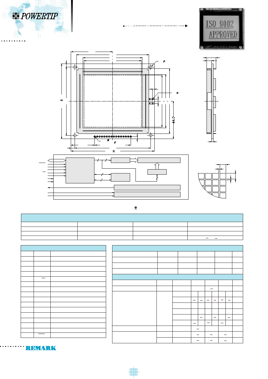
OUTLINE DIMENSION & BLOCK DIAGRAM
PG 8080-A
PG 8080-A
MECHANICAL SPECIFICATION
Overall Size
View Area
Dot Size
Dot Pitch
88.0 x 88.0
62.7 x 62.7
0.66 x 0.66
0.76 x 0.76
Module
W /O B/L
EL B/L
LED B/L
H2 / H1
5.1 / 9.7
5.1 / 9.7
/
Vdd+0.3
V
V
V
16.5
7.0
Item
Supply for logic voltage
LCD driving supply voltage
Input voltage
Vdd-Vss
Vdd-Vee
Vin
25
o
C
25
o
C
25
o
C
-0.3
-0.3
-0.3
Symbol
Condition
Min.
Max.
Units
ABSOLUTE MAXIMUM RATING
Item
LCD operation voltage
LCM current consumption (No B/L)
Backlight current consumption
Symbol
Min.
Condition
Vop
Idd
LED/edge VB/L=4.2V
LED/array
Top
-20
o
C
0
o
C
25
o
C
40
o
C
70
o
C
VB/L=4.2V
N W
9.3
9.7
8.9
Vdd=5V
8.6
7.5
8
ELECTRICAL CHARACTERISTICS
Typical
N W
Max. Units
V
10.7
9.9
9.6
10.4
8.8
8.3
V
V
V
V
V
mA
mA
mA
N W
9.8
10.2
9.4
9.1
7.9
8.4
4
PIN ASSIGNMENT
Pin no.
Symbol
Function
1
2
3
4
5
6
7
8
9
10
11
12
13
14
Vss
Vdd
Vo
Ao
R/W
E
DB0
DB1
DB2
DB3
DB4
DB5
DB6
DB7
Power supply(GND)
Power supply(+)
Contrast Adjust
Command / data select
Data read / write
Enable signal
Data bus line
Data bus line
Data bus line
Data bus line
Data bus line
Data bus line
Data bus line
Data bus line
15
16
Vee
RST
Negative voltage
Reset
25
o
C
Power supply voltage
Vdd-Vss
4.5
5.5
V
2.8
DB0~DB7
Vo
R/W
AO
Vss
A
K
RST
E
Vdd
Vee
LC7981
LCD PANEL
11
0.66
0.1
BACKLIGHT
2K RAM
COM
Negative Voltage Generator
8
5
3
8
80
4
80
COL
0
.
1
0
.
6
6
1.6
4
4
.
0
H2
H1
4- 3.0
4- 1.0
2.0
A
K
1
16- 1.0
PAD16- 1.8
P2.54 x 15=38.1
80.0
88.0 0.5
24.95
16
4.0
80 x 80 Dots
44.0
76.2
62.7
60.7
7
6
.
2
6
2
.
7
6
0
.
7
5
.
0
8
8
0
.
0
8
8
.
0
0
.
5
4
.
0
2
.
5