 | –≠–ª–µ–∫—Ç—Ä–æ–Ω–Ω—ã–π –∫–æ–º–ø–æ–Ω–µ–Ω—Ç: NJU8710 | –°–∫–∞—á–∞—Ç—å:  PDF PDF  ZIP ZIP |
NJU8710
- 1 -
Ver.2004-06-02
2V Operation Clock-less Switching Driver for Class D Amplifier
GENERAL DESCRIPTION
The
NJU8710
is a 2V operation clock-less switching
driver for a class D Amplifier with separated power supply
between Input and Output.
The
NJU8710
provides powerful drivability in both of
sink and source without flow-through current. Therefore, it
can be used to the buffer or the switch as a driver IC.
Furthermore it converts 1bit digital signal input, such as
PWM or PDM signal, to analog signal output of the hi-fi
audio level through a simple external LC low-pass filter.
The
NJU8710
realizes very high power-efficiency
because of the class D operation and low voltage
operation. Therefore, it is suitable for battery powered
applications and others.
FEATURES
2-channel 1bit Digital Signal Input
Standby(Hi-Z) Control function
Operating Voltage
: 1.7V to 2.7V
Driving Voltage
: 1.7V to V
DD
CMOS Technology
Package Outline
: VSP10
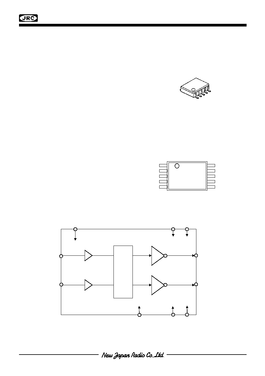
BLOCK DIAGRAM
PIN CONFIGURATION
PACKAGE OUTLINE
PRELIMINARY
NJU8710R
STBYB
IN
1
V
SS
V
DD
IN
2
V
SS
1
2
3
4
5
10
9
8
7
6
OUTX
1
V
DDO
OUTX
2
V
DDO
STBY
IN
2
IN
1
OUTX
1
OUTX
2
V
DD
V
SS
V
DDO
V
SS
V
DDO
Dead T
i
me
G
ener
ator

NJU8710
- 2 -
- 2 -
Ver.2004-06-02
TERMINAL DESCRIPTION
No.
SYMBOL
I/O
Function
10 V
DD
-
Power
Supply:
V
DD
=2V
5
6
V
DDO
-
Output Power Supply: V
DDO
=2V
3
8
V
SS
-
Power GND and Output GND terminal: V
SS
=0V
2
9
IN
1
IN
2
I
1-bit Data Input Terminal
4
7
OUTX
1
OUTX
2
O
Output Terminal
OUTX
1
terminal outputs the inverted signal of IN
1
terminal, OUTX
2
terminal outputs the inverted signal of IN
2
terminal.
1
STBYB
I Standby Control Terminal (L:Standby)
*V
SS
(Terminal No.3,8) should be connected at a nearest point to the IC.
*V
DDO
(Terminal No.5,6) should be connected at a nearest point to the IC.
*STBYB(Terminal No.1) must be connected to V
DD
, when this function is not used.
INPUT TERMINAL STRUCTURE
FUNCTIONAL DESCRIPTION
(1) Signal Output (OUTX
1
, OUTX
2
Terminal)
Output signal becomes a inverted input signal. A flow-through current at the signal polarity transition doesn't
generate by optimized dead time control circuit. Output signal is converted to analog signal via external
2nd-order or higher LC filter.
A switching regulator with a high response against a voltage fluctuation is the best selection for the V
DDO,
which is the power supply for output drivers. To obtain better T.H.D. performance, the stabilization of the power
is required.
(2) Standby Control Function
By setting the STBYB terminal to "L", the
NJU8710
becomes standby condition. During standby condition,
OUTX
1
and OUTX
2
are in Hi-Z.
V
DD
V
SS
Input
Terminal
IC Circuit
NJU3555
NJU8710
- 3 -
Ver.2004-06-02
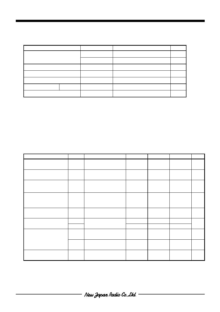
ABSOLUTE MAXIMUM RATINGS
(Ta=25
∞
C)
PARAMETER SYMBOL
RATING
UNIT
V
DD
-0.3
to
+4.0
V
Supply Voltage
V
DDO
-0.3
to
+2.7
V
Input Voltage
Vin
-0.3 to V
DD
+0.3 V
Operating Temperature
Topr
-40 to +85
∞
C
Storage Temperature
Tstg
-40 to +125
∞
C
Power Dissipation
VSP10
P
D
450*
mW
Power Supply Voltage Condition
- V
DD
V
DDO
V
* : Mounted on two-layer board of based on the JEDEC.
Note 1) All voltage values are specified as V
SS
=0V.
Note 2) If the LSI is used on condition beyond the absolute maximum rating, the LSI may be destroyed. Using
LSI within electrical characteristics is strongly recommended for normal operation. Use beyond the
electrical characteristics conditions will cause malfunction and poor reliability.
Note 3) De-coupling capacitors should be connected between V
DD
-V
SS
and V
DDO
-V
SS
due to the stabilized
operation.
ELECTRICAL CHARACTERISTICS
(Ta=25
∞
C, V
DD
=V
DDO
=2.0V, V
SS
=0.0V, unless otherwise noted)
PARAMETER SYMBOL
CONDITIONS
MIN. TYP. MAX.
UNIT
V
DD
Supply Voltage
V
DD
1.7 2.0 2.7
V
V
DDO
Supply Voltage
V
DDO
1.7
2.0
V
DD
V
Output Driver
High side Resistance
R
H
V
OUT
=V
DDO
-0.1V -
1.5
2
Output Driver
Low side Resistance
R
L
V
OUT
=0.1V -
1.5
2
Operating Current
at Hi-Z Output
I
ST
IN
1
, IN
2
, STBYB="L"
-
-
1
µ
A
I
DD
-
0.05
T.B.D
Operating Current
at no input signal
I
DDO
No-load operating,
IN
1
=IN
2
=1.4MHz
- 0.6
T.B.D
mA
V
IH
0.7V
DD
-
V
DD
V
Input Voltage
V
IL
0
-
0.3V
DD
V
Input Leakage Current
I
LK
-
-
±1
µ
A
NJU8710
- 4 -
- 4 -
Ver.2004-06-02
TIMING CHARACTERISTICS
∑
Signal Spread Characteristics
(Ta=25
∞
C, V
DD
=V
DDO
=2.0V, V
SS
=0.0V unless otherwise noted)
PARAMETER SYMBOL
CONDITIONS MIN. TYP. MAX.
UNIT
Maximum
Operating Frequency
f
Max
-
-
25 MHz
Signal Spread Time
(H L)
t
PDL
-
-
20
ns
Signal Spread Time
(L H)
t
PDH
-
-
20
ns
∑
Output Control Signal Input (STBYB)
(Ta=25
∞
C, V
DD
=V
DDO
=2.0V, V
SS
=0.0V unless otherwise noted)
PARAMETER SYMBOL
CONDITIONS MIN. TYP. MAX.
UNIT
Rise Time
t
UP
-
-
50
ns
Fall Time
t
DN
-
-
50
ns
OUTX
1
, OUTX
2
t
PDL
IN
1
, IN
2
t
PDH
0.7V
DD
0.3V
DD
0.7V
DD
0.3V
DD
t
DN
t
UP
STBYB
0.7V
DD
0.7V
DD
0.3V
DD
0.3V
DD
NJU3555
NJU8710
- 5 -
Ver.2004-06-02
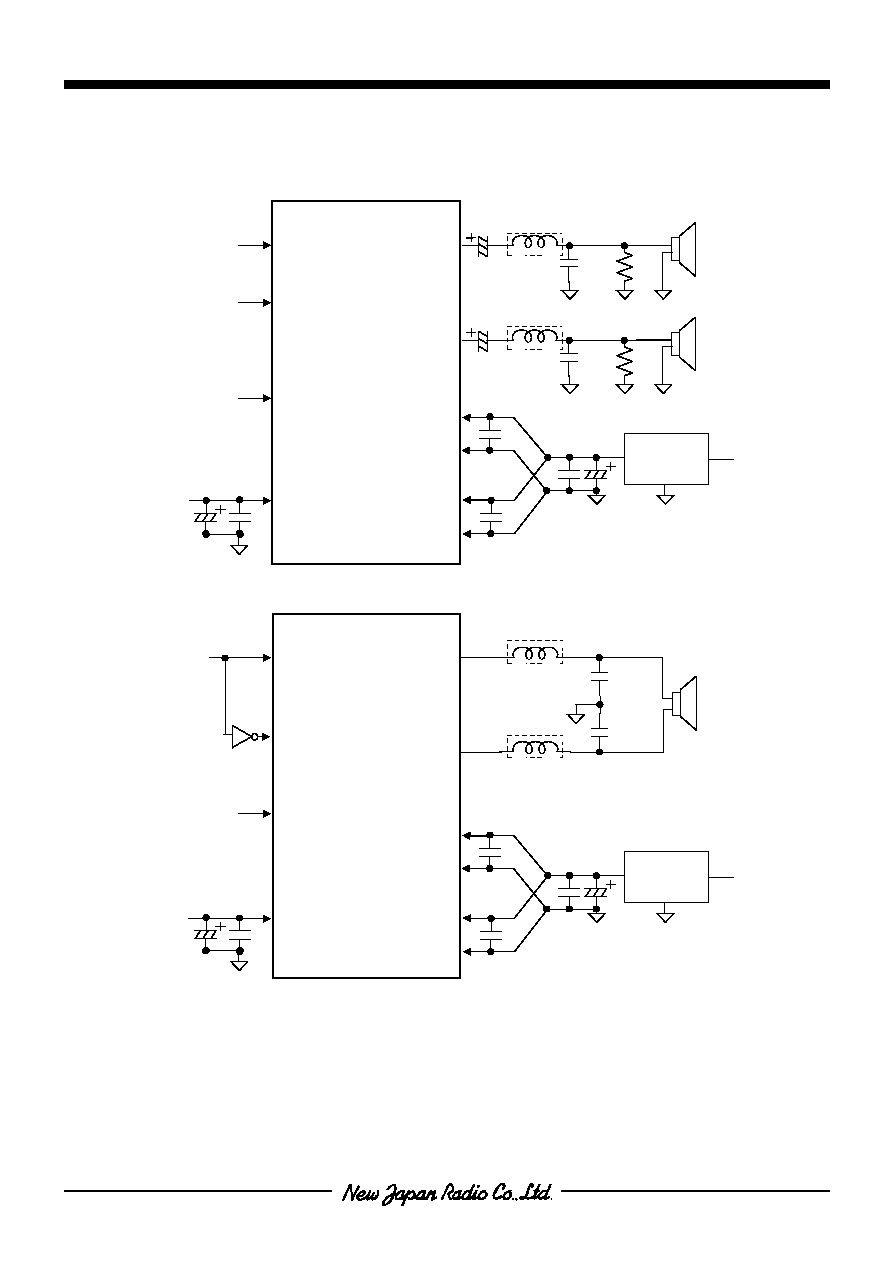
APPLICATION CIRCUIT (Analog Signal Output)
∑
Stereo OTL application example
∑
Monaural BTL application example
Note 4) De-coupling capacitors must be connected between each power supply terminal and GND terminal.
Note 5) The power supply for V
DDO
requires fast driving response performance such as a switching regulator for
T.H.D..
Note 6) The bigger capacitor value of external AC-coupling capacitors realize better low frequency response
characteristics. In addition, ESR(Equivalent Series Resistance) should be low.
Note 7) The above circuit shows only application example and does not guarantee the any electrical
characteristics. Therefore, please consider and check the circuit carefully to fit your application.
A914BY-101M
∑
A914BY-101M is manufactured by TOKO, INC.
For further information, please refer to its
technical papers.
A914BY-101M
NJU8
710
IN
1
OUTX
1
Standby Control
OUTX
2
Audio Signal
IN
2
STBYB
Headphone
32
0.
22
µ
F
100
µ
H
220
µ
F
1k
0.
22
µ
F
100
µ
H
220
µ
F
1k
2
9
1
4
7
V
DDO
0.1
µ
F
V
SS
5
3
V
DDO
0.1
µ
F
V
SS
6
8
47
µ
F
Switching
Regulato
r
0.1
µ
F
10
Logic Power
V
DD
0.1
µ
F
10
µ
F
A914BY-101M
IN
1
Audio Signal
IN
2
Speaker
32
0.
22
µ
F
100
µ
H
0.
22
µ
F
100
µ
H
0.1
µ
F
0.1
µ
F
47
µ
F
Switching
Regulato
r
0.1
µ
F
Standby Control
Logic Power
0.1
µ
F
10
µ
F
A914BY-101M
OUTX
1
OUTX
2
STBYB
2
9
1
4
7
V
DDO
V
SS
5
3
V
DDO
V
SS
6
8
10
V
DD
NJU8
710
∑
A914BY-101M is manufactured by TOKO, INC.
For further information, please refer to its
technical papers.