
41
P4C1681, P4C1682
P4C1681, P4C1682
ULTRA HIGH SPEED 4K x 4
STATIC CMOS RAMS
FEATURES
Full CMOS, 6T Cell
High Speed (Equal Access and Cycle Times)
≠ 12/15/20/25 ns (Commercial)
≠ 20/25/35ns (P4C1682 Military)
Low Power Operation (Commercial)
≠ 715 mW Active ≠ 12, 15
≠ 550 mW Active ≠ 20/25/35
≠ 193 mW Standby (TTL Input)
≠ 83 mW Standby (CMOS Input)
Single 5V
±
10%Power Supply
Separate Inputs and Outputs
≠ P4C1681 Input Data at Outputs during Write
≠ P4C1682 Outputs in High Z during Write
Fully TTL Compatible Inputs and Outputs
Standard Pinout (JEDEC Approved)
≠ 24-Pin 300 mil DIP
≠ 24-Pin 300 mil SOIC
≠ 24-Pin 300 mil SOJ
≠ 24-Pin CERDIP
≠ 28-Pin LCC (450 mil x 450 mil)
.
DESCRIPTION
The P4C1681 and P4C1682 are 16,384-bit (4K x 4) ultra
high speed static RAMs similar to the P4C168, but with
separate data I/O pins. The P4C1681 features a
transparent write operation; the outputs of the P4C1682
are in high impedance during the write cycle. All devices
have low power standby modes. The RAMs operate from
a single 5V
±
10% tolerance power supply.
Access times as fast as 12 nanoseconds are available,
permitting greatly enhanced system operating speeds.
CMOS is used to reduce power consumption to a low 715
mW active, 193 mW standby. For the P4C1682 and
P4C1681, power is only 83 mW standby with CMOS input
levels.
The P4C1681 and P4C1682 are available in 24-pin 300
mil DIP and SOIC packages providing excellent board
level densities. The P4C1682 is also available in a 28-pin
LCC package.
FUNCTIONAL BLOCK DIAGRAM
PIN CONFIGURATIONS
A
INPUT
DATA
CONTROL
ROW
SELECT
16,384-BIT
MEMORY
ARRAY
COLUMN I/O
A
A
A
(7)
(5)
I
1
I
2
I
3
I
4
COLUMN
SELECT
P4C1682
P4C1681
CE
O
1
O
2
O
3
O
4
WE
POWER
DOWN
1Q97
Means Quality, Service and Speed
DIP (P4,D4), SOIC (S4), SOJ (J4)
TOP VIEW
LCC (L5-1)
TOP VIEW
A7
A6
NC
NC
A5
O4
5
6
7
8
9
1 0
11
23
22
21
20
19
24
25
A9
A8
I3
I1
GND
CE
WE
O
1
A4
1
2
4
2 8
2 6
1 2
1 3 1 4 1 5
1 8
I 2
A
1
A
0
V
CC
A
11
A
2
3
2 7
1 6
1 7
A
3
A
10
O
2
O
3
NC
NC
I4
I 3
A0
A1
A2
A3
A4
A5
A6
A7
I1
I2
1
2
3
4
5
6
7
8
9
10
11
12
24
23
22
21
20
19
18
17
16
15
14
13
CE
GND
VCC
A11
A10
A9
A8
O4
WE
O2
O1
I4
O3

42
P4C1681, P4C1682
MAXIMUM RATINGS
1
Symbol
Parameter
Value
Unit
V
CC
Power Supply Pin with
≠0.5 to +7
V
Respect to GND
Terminal Voltage with
≠0.5 to
V
TERM
Respect to GND
V
CC
+0.5
V
(up to 7.0V)
T
A
Operating Temperature
≠55 to +125
∞
C
Symbol
Parameter
Value
Unit
T
BIAS
Temperature Under
≠55 to +125
∞
C
Bias
T
STG
Storage Temperature
≠65 to +150
∞
C
P
T
Power Dissipation
1.0
W
I
OUT
DC Output Current
50
mA
P4C1681
P4C1682
Sym.
V
IH
V
IL
V
HC
V
LC
V
CD
V
OL
V
OLC
V
OH
V
OHC
I
LI
I
LO
Parameter
Input High Voltage
Input Low Voltage
CMOS Input High Voltage
CMOS Input Low Voltage
Input Clamp Diode Voltage
Output Low Voltage
(TTL Load)
Output Low Voltage
(CMOS Load)
Output High Voltage
(TTL Load)
Output High Voltage
(CMOS Load)
Input Leakage Current
Output Leakage Current
Test Conditions
V
CC
= Min., I
IN
= ≠18 mA
I
OL
= +8 mA, V
CC
= Min.
I
OLC
= +100
µ
A, V
CC
= Min.
I
OH
= ≠4 mA, V
CC
= Min.
I
OHC
= ≠100
µ
A, V
CC
= Min.
V
CC
= Max. Mil.
V
IN
= GND to V
CC
Comm'l
V
CC
= Max. Mil.
CE
= V
IH
Comm'l
V
OUT
= GND to V
CC
Min
2.2
≠0.5
(3)
V
CC
≠0.2
≠0.5
(3)
2.4
V
CC
≠0.2
≠10
≠5
≠10
≠5
Max
V
CC
+0.5
0.8
V
CC
+0.5
0.2
≠1.2
0.4
0.2
+10
+5
+10
+5
Unit
V
V
V
V
V
V
V
V
V
µ
A
µ
A
µ
A
µ
A
DC ELECTRICAL CHARACTERISTICS
Over Recommended operating temperature and supply voltages(2)
RECOMMENDED OPERATING
TEMPERATURE AND SUPPLY VOLTAGE
Grade(2)
Ambient
Temperature
GND
V
CC
0V
5.0V
±
10%
≠55
∞
C to +125
∞
C
Military
Symbol
C
IN
C
OUT
Parameter
Input Capacitance
Output Capacitance
Conditions
V
IN
= 0V
V
OUT
= 0V
5
7
Unit
pF
pF
CAPACITANCES
(4)
V
CC
= 5.0V, T
A
= 25
∞
C, f = 1.0MHz
Typ.
5.0V
±
10%
0
∞
C to +70
∞
C
Commercial
0V
Notes:
1. Stresses greater than those listed under MAXIMUM RATINGS may
cause permanent damage to the device. This is a stress rating only
and functional operation of the device at these or any other conditions
above those indicated in the operational sections of this specification
is not implied. Exposure to MAXIMUM rating conditions for extended
periods may affect reliability.
2. Extended temperature operation guaranteed with 400 linear feet per
minute of air flow.
3. Transient inputs with V
IL
and I
IL
not more negative than ≠3.0V and
≠100mA, respectively, are permissible for pulse widths up to 20 ns.
4. This parameter is sampled and not 100% tested.

43
P4C1681, P4C1682
Symbol
Parameter
Test Conditions
Unit
POWER DISSIPATION CHARACTERISTICS
Over recommended operating temperature and supply voltage
(2)
P4C1681
P4C1682
Min
Max
I
CC
Dynamic Operating
V
CC
= Max., f = Max.,
Current ≠ 12, 15
Outputs Open Comm'l
--
130
mA
I
CC
Dynamic Operating
V
CC
= Max., f = Max., Mil.
≠
130
mA
Current ≠ 20, 25, 35
Outputs Open Comm'l
--
100
mA
I
SB
Standby Power Supply
CE
V
IH
,
Current (TTL Input Levels)
V
CC
= Max.,
--
35
mA
f = Max., Outputs Open
I
SB1
Standby Power Supply
CE
V
HC
,
Current
V
CC
= Max.,
--
15
mA
(CMOS Input Levels)
f = 0, Outputs Open,
V
IN
V
LC
or V
IN
V
HC
44
P4C1681, P4C1682
Notes:
5.
WE
is HIGH for READ cycle.
6.
CE
,
OE
are LOW for READ cycle.
7. ADDRESS must be valid prior to, or coincident with,
CE
transition LOW.
-12
-15
-20
-25
-35
Min
Max
Min
Max
Min Max
Min
Max Min
Max
t
RC
Read Cycle Time
12
15
20
25
35
ns
t
AA
Address Access
12
15
20
25
35
ns
Timens
t
AC
Chip Enable
12
15
20
25
35
ns
Access Time
t
OH
Output Hold from
2
2
3
3
3
ns
Address Change
t
LZ
Chip Enable to
2
2
3
3
3
ns
Output in Low Z
t
HZ
Chip Disable to
6
7
9
10
15
ns
Output in High Z
t
RCS
Read Command
0
0
0
0
0
ns
Setup Time
t
RCH
Read Command
0
0
0
0
0
ns
Hold Time
t
PU
Chip Enable to
0
0
0
0
0
ns
Power Up Time
t
PD
Chip Disable to
12
15
20
25
25
ns
Power Down Time
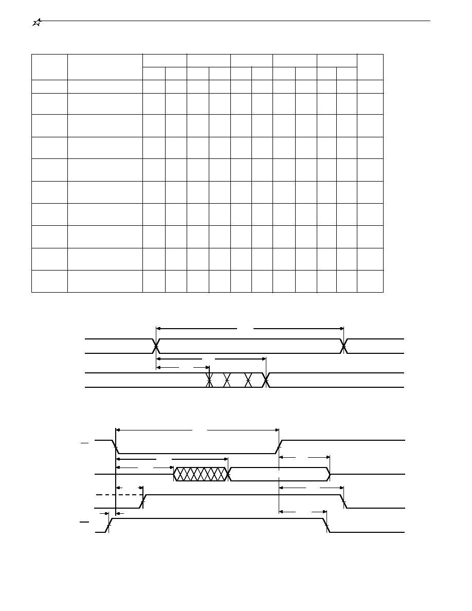
READ CYCLE NO. 1 (ADDRESS controlled)
(5, 6)
READ CYCLE NO. 2 (
CE
CE
CE
CE
CE
controlled)
(5, 7)
8. Transition is measured
±
200mV from steady state voltage prior to
change, with loading as specified in Figure 1.
9. Read Cycle Time is measured from the last valid address to the first
transitioning address.
Symbol
Parameter
Unit
AC ELECTRICAL CHARACTERISTICS--READ CYCLE
(V
CC
= 5V
±
10%, All Temperature Ranges)
(2)
1552 Tbl 10
t
DATA OUT
AC
t
RC
t
LZ
DATA VALID
I
CC
I
SB
t
PU
HIGH IMPEDANCE
t
PD
(3)
(8)
t
HZ
SUPPLY
CC
CURRENT
V
CE
t
RCS
t
RCH
WE
t
ADDRESS
DATA OUT
AA
t
t
OH
DATA VALID
PREVIOUS DATA VALID
(9)
RC
45
P4C1681, P4C1682
-12
-15
-20
-25
-35
Min
Max
Min
Max
Min Max
Min
Max Min
Max
t
WC
Write Cycle Time
12
15
18
20
30
ns
t
CW
Chip Enable Time
12
15
18
20
25
ns
to End of Write
t
AW
Address Valid to
12
15
18
20
25
ns
End of Write
t
AS
Address Set-up
0
0
0
0
0
ns
Time
t
WP
Write Pulse Width
12
15
18
20
25
ns
t
AH
Address Hold
0
0
0
0
0
ns
Time
t
DW
Data Valid to
7
8
10
10
15
ns
End of Write
t
DH
Data Hold Time
0
0
0
0
0
ns
t
WZ
Write Enable to
4
5
7
7
13
ns
Output in High Z
t
OW
Output Active to
0
0
0
0
0
ns
End of Write
t
AWE
Write Enable to
12
15
20
25
30
ns
Data-out Valid
£
t
ADV
Data-in Valid to
12
15
20
25
30
ns
Data-out Valid
P4C1682 only.
£
P4C1681 only.
AC ELECTRICAL CHARACTERISTICS--WRITE CYCLE
(V
CC
= 5V
±
10%, All Temperature Ranges)
(2)
12. Write Cycle Time is measured from the last valid address to the
first transitioning address.
10.
CE
and
WE
must be LOW for WRITE cycle.
11. If
CE
goes HIGH simultaneously with
WE
HIGH, the output
remains in a high impedance state.
Symbol
Parameter
Unit
WRITE CYCLE NO. 1 (
WE
WE
WE
WE
WE
controlled)
(10)
t
ADDRESS
t
WC
DATA VALID
HIGH IMPEDANCE
WE
DATA IN
DATA OUT
P4C1682
DATA UNDEFINED
(12)
(8)
t
CW
t
AW
t
WP
t
DW
t
WR
t
AH
t
DH
t
OW
t
AS
WZ
(8,11)
t
AWE
DATA VALID
DATA OUT
P4C1681
t
ADV
CE
(8)
Notes:
46
P4C1681, P4C1682
SELECTION GUIDE
The P4C1681 and P4C1682 are available in the following temperature, speed and package options.
Temperature
Range
Commercial
Plastic DIP
SOIC
SOJ
Speed (ns)
12
-12PC
-12SC
-12JC
15
-15PC
-15SC
-15JC
20
-20PC
-20SC
-20JC
25
-25PC
-25SC
-25JC
35
N/A
N/A
N/A
Package
Military
Processed*
(P4C1682 Only)
N/A
N/A
-20LMB
-20DMB
-25LMB
-25DMB
Military Temp.
LCC
CERDIP
N/A
N/A
-35LMB
-35DMB
LCC
CERDIP
N/A
N/A
N/A
N/A
-20LM
-20DM
-25LM
-25DM
-35LM
-35DM
* Military temperature range with MIL-STD-883 Revision D, Class B processing.
N/A = Not available
ORDERING INFORMATION
P4C
Static RAM Prefix
1682
l
--
ss
p
t
Temperature Range
Package Code
Speed (Access/Cycle Time)
Low Power Designator
Blank = None; L = Low Power
Device Number
= Ultra-low standby power designator L, if available.
= Speed (access/cycle time in ns), e.g., 25, 35
= Package code, i.e., P, D, S, L.
= Temperature range, i.e., C, M, MB.
l
ss
p
t
P4C
1681
PACKAGE SUFFIX
Package
Suffix
P
Plastic DIP, 300 mil wide standard
J
Plastic SOJ
D
CERDIP, 300 mil wide standard
S
Small Outline IC
L
LCC Package
Description
Description
TEMPERATURE RANGE SUFFIX
Temperature
Range Suffix
C
Commercial Temperature Range,
≠0
∞
C to +70
∞
C.
M
Military Temperature Range,
≠55
∞
C to +125
∞
C.
MB
Mil. Temp. with MIL-STD-883C
Class D compliance
(P4C1682 Only)