
33
P4C168, P4C169, P4C170
P4C168, P4C169, P4C170
ULTRA HIGH SPEED 4K x 4
STATIC CMOS RAMS
DESCRIPTION
The P4C168, P4C169 and P4C170 are a family of 16,384-
bit ultra high-speed static RAMs organized as 4K x 4. All
three devices have common input/output ports.The
P4C168 enters the standby mode when the chip enable
(
CE
) control goes high; with CMOS input levels, power
consumption is only 83mW in this mode. Both the P4C169
and the P4C170 offer a fast chip select access time that is
only 67% of the address access time. In addition, the
P4C170 includes an output enable (
OE
) control to elimi-
nate data bus contention. The RAMs operate from a single
5V
±
10% tolerance power supply.
FEATURES
Full CMOS, 6T Cell
High Speed (Equal Access and Cycle Times)
≠ 12/15/20/25ns (Commercial)
≠ 20/25/35ns (P4C168 Military)
Low Power Operation (Commercial)
≠ 715 mW Active
≠ 193 mW Standby (TTL Input) P4C168
≠ 83 mW Standby (CMOS Input) P4C168
Single 5V
±
10% Power Supply
Fully TTL Compatible, Common I/O Ports
Three Options
≠ P4C168 Low Power Standby Mode
≠ P4C169 Fast Chip Select Control
≠ P4C170 Fast Chip Select, Output Enable
Controls
Standard Pinout (JEDEC Approved)
≠ P4C168: 20-pin DIP, SOJ and SOIC
≠ P4C169: 20-pin DIP and SOIC
≠ P4C170: 22-pin DIP
Access times as fast as 12 nanoseconds are available,
permitting greatly enhanced system operating speeds.
CMOS is used to reduce power consumption to a low 715
mW active, 193 mW standby.
The P4C168 and P4C169 are available in 20-pin (P4C170
in 22-pin) 300 mil DIP packages providing excellent board
level densities. The P4C168 is also available in 20-pin 300
mil SOIC and SOJ packages.
The P4C169 is also available in a 20-pin 300 mil SOIC
package. The P4C170 is also available in a 22-pin 300 mil
SOJ package.
PIN CONFIGURATIONS
FUNCTIONAL BLOCK DIAGRAM
1Q97
Means Quality, Service and Speed
INPUT
DATA
CONTROL
ROW
SELECT
16,384-BIT
MEMORY
ARRAY
COLUMN I/O
I/O
1
I/O
2
I/O
3
I/O
4
COLUMN
SELECT
POWER
DOWN
P4C168
ONLY
or
(7)
A
CE
A
CS
OE
WE
A
A
(5)
NOTES:
CE
USED ON P4C168 ALSO FOR POWER DOWN FUNCTIONS
CE
USED ON P4C169 FAST CHIP SELECT
OE
OUTPUT ENABLE FUNCTION ON P4C170 ONLY
P4C168 P4C169
DIP (P2, D2) DIP (P2)
SOIC (S2) SOIC (S2)
SOJ (J2)
TOP VIEW
P4C170
DIP (P3)
TOP VIEW
A
4
A
7
A
0
A
1
A
2
A
3
A
5
A
6
A
11
A
1 0
A
9
A
8
NC
I/O
4
V
C C
CS
GND
1
2
3
4
5
6
7
8
9
1 0
11
22
21
20
19
18
17
16
15
14
13
12
OE
I/O
3
I/O
2
I/O
1
WE
A
4
A
7
A
0
A
1
A
2
A
3
A
5
A
6
A
11
A
1 0
A
9
A
8
I/O
4
V
C C
CE
,
CS
GND
1
2
3
4
5
6
7
8
9
1 0
20
19
18
17
16
15
14
13
12
11
I/O
3
I/O
2
I/O
1
WE

P4C168, P4C169, P4C170
34
MAXIMUM RATINGS
(1)
Symbol
Parameter
Value
Unit
V
CC
Power Supply Pin with
≠ 0.5 to +7
V
Respect to GND
Terminal Voltage with
≠ 0.5 to
V
TERM
Respect to GND
V
CC
+0.5
V
(up to 7.0V)
T
A
Operating Temperature
≠55 to +125
∞
C
Symbol
Parameter
Value
Unit
T
BIAS
Temperature Under
≠ 55 to +125
∞
C
Bias
T
STG
Storage Temperature
≠ 65 to +150
∞
C
P
T
Power Dissipation
1.0
W
I
OUT
DC Output Current
50
mA
Symbol
Parameter
Conditions Typ. Unit
C
IN
Input Capacitance
V
IN
= 0V
5
pF
C
OUT
Output Capacitance V
OUT
= 0V
7
pF
RECOMMENDED OPERATING CONDITIONS
CAPACITANCES
(4)
(V
CC
= 5.0V, T
A
= 25
∞
C, f = 1.0MHz)
Grade
(2)
Commercial
Military
Ambient Temp
0
∞
C to 70
∞
C
≠55
∞
C to +125
∞
C
Gnd
0V
0V
V
CC
5.0V
±
10%
5.0V
±
10%
V
IH
V
IL
V
HC
V
LC
V
OH
I
LI
I
SB
I
SB1
Input High Voltage
Input Low Voltage
CMOS Input High Voltage
CMOS Input Low Voltage
Output Low Voltage
(TTL Load)
Output High Voltage
(CMOS Load)
Input Leakage Current
Output Leakage Current
Dynamic Operating
Current
Standby Power Supply
Current (TTL Input Levels)
P4C168 only
Standby Power
Supply Current
(CMOS Input Levels)
P4C168 only
Input Clamp Diode Voltage
Output Low Voltage
(CMOS Load)
Output High Voltage
(TTL Load)
Parameter
Symbol
Test Conditions
V
CC
= Min., I
IN
= ≠18 mA
V
CC
= Max., V
IN
= GND to V
CC
V
CC
= Max.,
CS
= V
IH
,
V
OUT
= GND to V
CC
CE
V
IH
, V
CC
= Max., f = Max.,
Outputs Open
CE
V
HC
, V
CC
= Max., f = 0,
Outputs Open
V
IN
V
LC
or V
IN
V
HC
Mil.
Comm'l
Mil.
Comm'l
P4C168/169/170
Min
2.2
≠0.5(3)
V
CC
≠0.2
≠0.5(3)
2.4
≠10
≠5
≠10
≠5
Max
V
CC
+0.5
0.8
V
CC
+0.5
0.2
+10
+5
+10
+5
Unit
V
V
V
V
≠1.2
V
V
CD
I
OL
= +8 mA, V
CC
= Min.
0.4
V
V
OL
I
OLC
= +100
µ
A, V
CC
= Min.
0.2
V
V
OLC
I
OH
= ≠4 mA, V
CC
= Min.
V
I
OHC
= ≠100
µ
A, V
CC
= Min.
V
CC
≠0.2
V
V
OHC
µ
A
I
LO
µ
A
I
CC
35
mA
15
mA
___
___
V
CC
= Max., f = Max., Outputs Open
130
mA
___
DC ELECTRICAL CHARACTERISTICS
35
P4C168, P4C169, P4C170
AC CHARACTERISTICS--READ CYCLE
(V
CC
= 5V
±
10%, All Temperature Ranges)
(2)
Sym.
t
RC
t
AA
Parameter
Read Cycle Time
Address Access Time
≠12
≠15
≠20
≠25
Min Max Min Max Min Max Min Max Min Max
≠35
Unit
12
12
15
15
20
25
35
ns
ns
20
25
35
Chip Enable Access Time
t
AC
ß
12
15
20
25
35
ns
Chip Select Access Time
t
AC
8
9
12
15
20
ns
t
OH
Output Hold from Address Change
2
2
2
2
2
ns
Chip Enable to Output in Low Z
t
LZ
2
2
2
2
2
ns
Chip Disable to Output in High Z
t
HZ
6
7
9
10
15
ns
Output Enable to Data Valid
t
OE
8
12
10
15
15
ns
Output Enable to Output in Low Z
t
OLZ
0
0
0
0
0
ns
Output Disable to Output in High Z
t
OHZ
6
7
9
11
15
ns
Read Command Setup Time
t
RCS
0
0
0
0
0
ns
Read Command Hold Time
t
RCH
0
0
0
0
0
ns
Chip Enable to Power Up Time
t
PU
ß
0
0
0
0
0
ns
Chip Disable to Power Down Time
t
PD
ß
12
15
20
25
35
ns
ß P4C168 only
P4C170 only
Chip Select/Deselect for P4C169 and P4C170
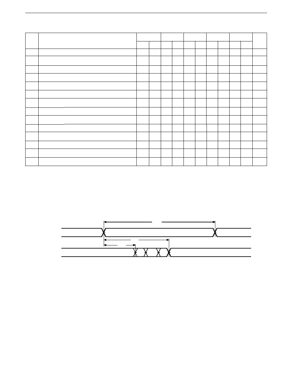
TIMING WAVEFORM OF READ CYCLE NO. 1 (ADDRESS CONTROLLED)
(5,6)
t
ADDRESS
DATA OUT
AA
t
t
OH
DATA VALID
PREVIOUS DATA VALID
(9)
RC
Notes:
5.
WE
is HIGH for READ cycle.
6.
CE
/
CS
and
OE
are LOW for READ cycle.

P4C168, P4C169, P4C170
36
Notes:
7. ADDRESS must be valid prior to, or coincident with
CE
/
CS
transition
low. For Fast
CS
, t
AA
must still be met.
8. Transition is measured
±
200mV from steady state voltage prior to
change, with loading as specified in Figure 1.
9. Read Cycle Time is measured from the last valid address to the first
transitioning address.
TIMING WAVEFORM OF READ CYCLE NO. 2 (
CE
CE
CE
CE
CE
/
CS
CS
CS
CS
CS
CONTROLLED)
(5,7)
TIMING WAVEFORM OF READ CYCLE NO. 3--P4C170 ONLY (
OE
OE
OE
OE
OE
CONTROLLED)
(5)
ADDRESS
t
RC
(9)
1521 05
OE
t
AA
t
CS
OE
t
OH
t
AC
t
OHZ
t
(8)
(8)
DATA OUT
t
HZ
t
LZ
(8)
(8)
OLZ
READ CYCLE WAVEFORM NO. 2 (
CS
Controlled)
t
CE
/
CS
DATA OUT
AC
t
RC
t
LZ
(5,7)
DATA VALID
t
OLZ
HIGH IMPEDANCE
(7)
(7)
t
HZ
(7)
t
OHZ
OE
(7)
I
CC
I
SB
t
PU
t
PD
SUPPLY
CC
CURRENT
V
WE
(P4C170)
(P4C168 ONLY)
t
RCS
t
RCH
t
OE

37
P4C168, P4C169, P4C170
Notes:
10.
CE
/
CS
and
WE
must be LOW for WRITE cycle.
11. If
CE
/
CS
goes HIGH simultaneously with
WE
HIGH, the output
remains in a high impedance state.
12. Write Cycle Time is measured from the last valid address to the first
transitioning address.
ADDRESS
CE/CS
t
WC
DATA VALID
HIGH IMPEDANCE
WE
DATA IN
DATA OUT
DATA UNDEFINED
(12)
(8)
t
CW
t
AW
t
WP
t
DW
t
WR
t
AH
t
DH
t
OW
t
AS
t
WZ
(8,11)
TIMING WAVEFORM OF WRITE CYCLE NO. 1 (
WE
WE
WE
WE
WE
CONTROLLED)
(10)
AC ELECTRICAL CHARACTERISTICS - WRITE CYCLE
(V
CC
= 5V
±
10%, All Temperature Ranges)
(2)
Sym.
Parameter
Write Cycle Time
Chip Enable Time to
End of Write
Address Valid to
End of Write
Address Set-up Time
Write Pulse Width
Address Hold Time
Data Valid to End
of Write
Data Hold Time
Write Enable to
Output in High Z
Output Active from
End of Write
t
WC
t
CW
t
WP
t
AH
t
DW
t
DH
t
WZ
t
AS
t
OW
≠12
≠15
t
AW
≠20
≠25
≠35
Min
12
12
12
12
0
7
0
0
4
Max Min
15
15
15
0
15
0
8
0
0
Max
5
Min
18
18
18
0
18
0
10
0
0
Max
7
Min
20
20
20
0
0
10
0
0
20
Max
7
Min
35
30
30
0
30
0
15
0
0
Max
Unit
ns
ns
ns
ns
ns
ns
ns
0
ns
ns
13
ns