71
P4C198/198L, P4C198A/198AL
P4C198/P4C198L, P4C198A/P4C198AL
ULTRA HIGH SPEED 16K x 4
STATIC CMOS RAMS
FEATURES
Full CMOS, 6T Cell
High Speed (Equal Access and Cycle Times)
≠ 10/12/15/20/25 ns (Commercial)
≠ 12/15/20/25/35 ns (Industrial)
≠ 15/20/25/35/45 ns (Military)
Low Power Operation (Commercial/Military)
≠ 715 mW Active ≠ 12/15
≠ 550/660 mW Active ≠ 20/25/35/45/55
≠ 193/220 mW Standby (TTL Input)
≠ 83/110 mW Standby (CMOS Input) P4C198/198A
≠ 9 mW Standby (CMOS Input)
P4C198L/198AL (Military)
5V
±
10% Power Supply
Data Retention, 10
µ
A Typical Current from 2.0V
P4C198L/198AL (Military)
Output Enable & Chip Enable Control Functions
≠ Single Chip Enable P4C198
≠ Dual Chip Enable P4C198A
Common Inputs and Outputs
Fully TTL Compatible Inputs and Outputs
Standard Pinout (JEDEC Approved)
≠ 24-Pin 300 mil DIP
≠ 24-Pin 300 mil SOJ (P4C198 only)
≠ 28-Pin 350 x 550 mil LCC (P4C198 only)
(P4C198A ONLY)
A
CE
WE
INPUT
DATA
CONTROL
ROW
SELECT
65,536-BIT
MEMORY
ARRAY
COLUMN I/O
A
A
A
(8)
(6)
I/O
1
I/O
2
I/O
3
I/O
4
COLUMN
SELECT
(CE )
1
(CE )
2
OE
1Q97
Means Quality, Service and Speed
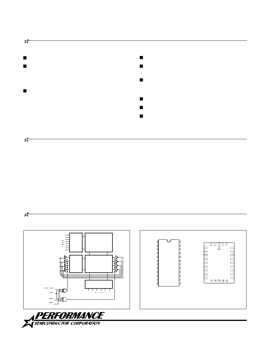
FUNCTIONAL BLOCK DIAGRAM
PIN CONFIGURATIONS
The P4C198/L and P4C198A/L are 65,536-bit ultra high-
speed static RAMs organized as 16K x 4. Each device
features an active low Output Enable control to eliminate
data bus contention. The P4C198/L also have an active
low Chip Enable (the P4C198A/L have two Chip Enables,
both active low) for easy system expansion. The CMOS
memories require no clocks or refreshing and have equal
access and cycle times. Inputs are fully TTL-compatible.
The RAMs operate from a single 5V
±
10% tolerance
power supply. Data integrity is maintained with supply
DESCRIPTION
voltages down to 2.0V. Current drain is typically 10
µ
A
from a 2.0V supply.
Access times as fast as 12 nanoseconds are available,
permitting greatly enhanced system operating speeds.
CMOS is used to reduce power consumption to a low 715
mW active, 193 mW standby.
The P4C198/L and P4C198A/L are available in 24-pin 300
mil DIP and SOJ, and 28-pin 350 x 550 mil LCC packages
providing excellent board level densities.
DIP (P4, D4), SOJ (J4)
TOP VIEW
P4C198 (P4C198A)
LCC (L5)
TOP VIEW
P4C198 ONLY
I/O2
C E
A7
A6
A5
A4
A3
A2
A13
A12
A11
NC
4
5
6
7
8
9
10
11
12
24
23
22
21
20
19
18
25
26
A10
A9
2
28
A
0
NC
NC
V
CC
13
14 15 16
OE
GND
NC
WE
I/O
1
1
27
3
1 7
A1
A8
I/O3
I/O
NC
A4
A7
A0
A1
A2
A3
A5
A6
A13
A12
A11
A10
A9
NC (
C E
2)
I/O4
VCC
W E
GND
A8
OE
1
2
3
4
5
6
7
8
9
1 0
11
1 2
24
23
22
21
20
19
18
17
16
15
14
13
I/O3
I/O2
I/O1
C E
(
C E
1)

72
P4C198/198L, P4C198A/198AL
CE
1
,
CE
2
V
IH
Mil.
V
CC
= Max., Ind./Com'l.
f = 0, Outputs Open
V
IN
V
LC
or V
IN
V
HC
MAXIMUM RATINGS
(1)
Symbol
Parameter
Value
Unit
V
CC
Power Supply Pin with
≠0.5 to +7
V
Respect to GND
Terminal Voltage with
≠0.5 to
V
TERM
Respect to GND
V
CC
+0.5
V
(up to 7.0V)
T
A
Operating Temperature
≠55 to +125
∞
C
Symbol
Parameter
Value
Unit
T
BIAS
Temperature Under
≠55 to +125
∞
C
Bias
T
STG
Storage Temperature
≠65 to +150
∞
C
P
T
Power Dissipation
1.0
W
I
OUT
DC Output Current
50
mA
Notes:
1. Stresses greater than those listed under MAXIMUM RATINGS may
cause permanent damage to the device. This is a stress rating only
and functional operation of the device at these or any other conditions
above those indicated in the operational sections of this specification
is not implied. Exposure to MAXIMUM ratingconditions for extended
periods may affect reliability.
2. Extended temperature operation guaranteed with 400 linear feet per
minute of air flow.
3. Transient inputs with V
IL
and I
IL
not more negative than ≠3.0V and
≠100mA, respectively, are permissible for pulse widths up to 20 ns.
4. This parameter is sampled and not 100% tested.
RECOMMENDED OPERATING
TEMPERATURE AND SUPPLY VOLTAGE
I
SB
Standby Power Supply
Current (TTL Input Levels)
CE
1
,
CE
2
V
IH
Mil.
V
CC
= Max ., Ind./Com'l.
f = Max., Outputs Open
___
___
40
35
___
___
___
___
20
15
40
n/a
1.5
n/a
mA
mA
___
___
Standby Power Supply
Current
(CMOS Input Levels)
I
SB1
Commercial
Grade(2)
Ambient
Temperature
GND
V
CC
0
∞
C to +70
∞
C
≠40
∞
C to +85
∞
C
0V
0V
5.0V
±
10%
5.0V
±
10%
0V
5.0V
±
10%
≠55
∞
C to +125
∞
C
Military
Symbol
C
IN
C
OUT
Parameter
Input Capacitance
Output Capacitance
Conditions
V
IN
= 0V
V
OUT
= 0V
5
7
Unit
pF
pF
CAPACITANCES
(4)
V
CC
= 5.0V, T
A
= 25
∞
C, f = 1.0MHz
n/a = Not Applicable
Symbol
DC ELECTRICAL CHARACTERISTICS
Over recommended operating temperature and supply voltage
(2)
V
IH
V
IL
V
HC
V
LC
V
CD
V
OL
V
OH
I
LI
I
LO
Parameter
Input High Voltage
Input Low Voltage
CMOS Input High Voltage
CMOS Input Low Voltage
Input Clamp Diode Voltage
Output Low Voltage
(TTL Load)
Output High Voltage
(TTL Load)
Input Leakage Current
Output Leakage Current
Test Conditions
V
CC
= Min., I
IN
= 18 mA
I
OL
= +10 mA, V
CC
= Min.
I
OL
= +8 mA, V
CC
= Min.
I
OH
= ≠4 mA, V
CC
= Min.
V
CC
= Max. Mil.
V
IN
= GND to V
CC
Com'l.
V
CC
= Max.,
CE
= V
IH
, Mil.
V
OUT
= GND to V
CC
Com'l.
P4C198 / 198A
Min
2.2
≠0.5
(3)
V
CC
≠0.2
≠0.5
(3)
2.4
≠10
≠5
≠10
≠5
Max
V
CC
+0.5
0.8
V
CC
+0.5
0.2
≠1.2
0.4
+10
+5
+10
+5
P4C198L / 198AL
Min
Max
2.2
≠0.5
(3)
V
CC
≠0.2
≠0.5(3)
2.4
≠5
n/a
≠5
n/a
V
CC
+0.5
0.8
V
CC
+0.5
0.2
0.4
≠1.2
+5
n/a
+5
n/a
Unit
V
V
V
V
V
V
V
V
µ
A
µ
A
Typ.
Industrial
0.5
0.5

73
P4C198/198L, P4C198A/198AL
*V
CC
= 5.5V. Tested with outputs open. f = Max. Switching inputs are 0V and 3V.
198:
CE
= V
IL
,
OE
= V
IH
198A:
CE
1
= V
IL
,
CE
2
= V
IL
.
OE
= V
IH
DATA RETENTION CHARACTERISTICS (P4C198L/P4C198AL Military Temperature Only)
Typ.*
Max
Symbol
Parameter
Test Condition
Min
V
CC
=
V
CC
=
Unit
2.0V
3.0V
2.0V
3.0V
V
DR
V
CC
for Data Retention
2.0
V
I
CCDR
Data Retention Current
10
15
600
900
µ
A
t
CDR
Chip Deselect to
CE
V
CC
≠ 0.2V,
0
ns
Data Retention Time
V
IN
V
CC
≠ 0.2V or
t
R
Operation Recovery Time
t
RC
ß
ns
*
T
A
= +25
∞
C
ß
t
RC
= Read Cycle Time
This parameter is guaranteed but not tested.
V
IN
0.2V
DATA RETENTION WAVEFORM
V
CC
V
IH
t
CDR
4.5V
V
DR
2V
4.5V
t
R
V
DR
V
IH
DATA RETENTION MODE
CE
(
CE
, or CE
2
for the P4C198AL)
I
CC
Symbol
Parameter
Temperature
Range
Dynamic Operating Current*
Commercial
Industrial
Military
≠10
N/A
≠12
≠15
≠20
≠25
≠35
≠45
Unit
N/A
mA
mA
mA
POWER DISSIPATION CHARACTERISTICS VS. SPEED
N/A
150
155
160
170
180
N/A
170
160
155
150
145
180
170
160
155
150
N/A
N/A
74
P4C198/198L, P4C198A/198AL
Sym.
Parameter
Unit
-10
-12
-15
-20
-25
-35
-45
Min Max Min
Max
Min Max Min
Max Min Max Min
Max Min
Max
t
RC
Read Cycle Time
10
12
15
20
25
35
45
ns
t
AA
Address Access
10
12
15
20
25
35
45
ns
Time
t
AC
Chip Enable
10
12
15
20
25
35
45
ns
Access Time
t
OH
Output Hold from
2
2
2
2
2
2
2
ns
Address Change
t
LZ
Chip Enable to
2
2
2
2
2
2
2
ns
Output in Low Z
t
HZ
Chip Disable to
6
7
8
10
10
14
15
ns
Output in High Z
t
OE
Output Enable
6
7
9
12
15
25
30
ns
Low to Data Valid
t
OLZ
Output Enable to
2
2
2
2
2
2
2
ns
Output in Low Z
t
OHZ
Output Disable to
6
7
9
9
10
14
15
ns
Output in High Z
t
PU
Chip Enable to
0
0
0
0
0
0
0
ns
Power Up Time
t
PD
Chip Disable to
10
12
15
20
25
35
45
ns
Power Down Time
AC CHARACTERISTICS--READ CYCLE
(V
CC
= 5V
±
10%, All Temperature Ranges)
(2)
READ CYCLE NO.1 (
O E
O E
O E
O E
O E
controlled)
(5)
ADDRESS
O E
tRC
DATAOUT
(10)
tAA
tOE
tOH
C E
tOLZ
tAC
tLZ
tOHZ
tHZ
(9)
(9)
(9)
(9)
(12)
Notes:
5.
WE
is HIGH for READ cycle.
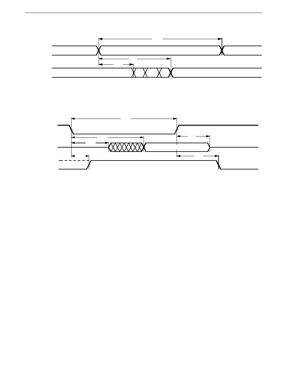
75
P4C198/198L, P4C198A/198AL
t
ADDRESS
DATA OUT
AA
t
t
OH
DATA VALID
PREVIOUS DATA VALID
(10)
RC
1520 05
READ CYCLE NO. 2 (ADDRESS Controlled)
(5,6)
READ CYCLE NO. 3 (
C E
C E
C E
C E
C E
(12)
Controlled)
(5,7,8)
10. Read Cycle Time is measured from the last valid address to
the first transitioning address.
11. Transitions caused by a chip enable control have similar
delays irrespective of whether
CE
1
or
CE
2
causes them
(P4C198A/L).
12.
CE
1
,
CE
2
for P4C198A/L.
Notes:
6.
CE
(
CE
1
CE
2
for P4C198A/L) and
OE
are LOW READ cycle.
7.
OE
is LOW for the cycle.
8. ADDRESS must be valid prior to, or coincident with
CE
(
CE
1
and
CE
2
for P4C198A/L) transition LOW.
9. Transition is measured
±
200mV from steady state voltage
prior to change, with loading as specified in Figure 1.
tAC
C E
DATA OUT
tRC
tLZ
DATA VALID
ICC
ISB
t
PU
HIGH IMPEDANCE
tPD
tHZ
CURRENT
VCC SUPPLY
(9,11)
(9,11)
(11)
(11)
(11)

76
P4C198/198L, P4C198A/198AL
-10
-12
-15
-20
-25
-35
-45
Min Max Min
Max
Min Max Min
Max Min Max Min
Max Min
Max
t
WC
Write Cycle Time
10
12
13
15
20
30
40
ns
t
CW
Chip Enable Time
7
8
10
15
20
30
35
ns
to End of Write
t
AW
Address Valid to
8
8
10
15
20
25
35
ns
End of Write
t
AS
Address Set-up
0
0
0
0
0
0
0
ns
Time
t
WP
Write Pulse
8
9
10
12
20
25
35
ns
Width
t
AH
Address Hold
0
0
0
0
0
0
0
ns
Time from End
of Write
t
DW
Data Valid to End
7
6
7
10
13
15
20
ns
of Write
t
DH
Data Hold Time
0
0
0
0
0
0
0
ns
t
WZ
Write Enable to
7
6
7
8
10
10
15
ns
Output in High Z
t
OW
Output Active
3
3
3
3
3
3
3
ns
from End of Write
AC CHARACTERISTICS--WRITE CYCLE
(V
CC
= 5V
±
10%, All Temperature Ranges)
(2)
Sym.
Parameter
Unit
OHZ
ADDRESS
CE
t
WC
HIGH IMPEDANCE
WE
DATA IN
DATA OUT
DATA UNDEFINED
1520 07
(16)
t
CW
t
AW
t
WP
t
DW
t
AH
t
DH
t
(12)
(9)
OE
t
AS
WRITE CYCLE NO. 1 (With
O E
O E
O E
O E
O E
high)

77
P4C198/198L, P4C198A/198AL
WRITE CYCLE NO. 2 (
W E
W E
W E
W E
W E
CONTROLLED)
(13,14)
1520 08
tDW
tAH
W E
ADDRESS
C E
(12)
DATA OUT
DATA IN
tWC
DATA VALID
HIGH IMPEDANCE
(16)
tAS
tCW
tAW
t
WP
tDH
tWR
WRITE CYCLE NO. 3 (
C E
C E
C E
C E
C E
(12)
CONTROLLED)
(13,14)
ADDRESS
C E
tWC
DATA VALID
HIGH IMPEDANCE
W E
DATA IN
DATA OUT
DATA UNDEFINED
(16)
(9)
tCW
tAW
tWP
tDW
tWR
tAH
tDH
tOW
tAS
tWZ
(9,15)
(11)
(12)
Notes:
13.
CE
(
CE
1
,
CE
2
for P4C198A/L) and
WE
must be LOW for WRITE
cycle.
14.
OE
is LOW for this WRITE cycle.
15. If
CE
(
CE
1
or
CE
2
for P4C198A/L) goes HIGH simultaneously with
WE
HIGH, the output remains in a high impedance state.
16. Write Cycle Time is measured from the last valid address to the first
transitioning address.

78
P4C198/198L, P4C198A/198AL
TRUTH TABLES
P4C198/L
P4C198A/L
C E
C E
C E
C E
C E
1
C E
C E
C E
C E
C E
2
W E
W E
W E
W E
W E
O E
O E
O E
O E
O E
Mode
Output
H
X
X
X
Standby
High Z
X
H
X
X
Standby
High Z
L
L
H
H
Output Inhibit
High Z
L
L
H
L
READ
D
OUT
L
L
L
X
WRITE
D
IN
C E
C E
C E
C E
C E
W E
W E
W E
W E
W E
O E
O E
O E
O E
O E
Mode
Output
H
X
X
Standby
High Z
L
H
H
Output Inhibit
High Z
L
H
L
READ
D
OUT
L
L
X
WRITE
D
IN
Input Pulse Levels
GND to 3.0V
Input Rise and Fall Times
3ns
Input Timing Reference Level
1.5V
Output Timing Reference Level
1.5V
Output Load
See Figures 1 and 2
* including scope and test fixture.
Note:
Because of the ultra-high speed of the P4C198/L and P4C198A/L, care
must be taken when testing this device; an inadequate setup can cause
a normal functioning part to be rejected as faulty. Long high-inductance
leads that cause supply bounce must be avoided by bringing the V
CC
and
ground planes directly up to the contactor fingers. A 0.01
µ
F high
Figure 1. Output Load
Figure 2. Thevenin Equivalent
frequency capacitor is also required between V
CC
and ground. To avoid
signal reflections, proper termination must be used; for example, a 50
test environment should be terminated into a 50
load with 1.73V
(Thevenin Voltage) at the comparator input, and a 116
resistor must be
used in series with D
OUT
to match 166
(Thevenin Resistance).
AC TEST CONDITIONS
DOUT
255
480
+5V
30pF* (5pF* for t
HZ
, t
LZ
t
WZ
OW
and t
,
)
30pF* (5pF* for tHZ, tLZ, tOHZ, tOLZ,
tWZ and tOW)
VTH = 1.73V
RTH = 166.5
DOUT
30pF* (5pF* for tHZ, tLZ, tOHZ, tOLZ,
tWZ and tOW)

79
P4C198/198L, P4C198A/198AL
* Military temperature range with MIL-STD-883, Class B processing.
N/A = Not available
SELECTION GUIDE
The P4C198 and P4C198A are available in the following temperature, speed and package options.
Temperature
Range
Military
Processed*
Commercial
Industrial
Military Temp.
Speed (ns)
Package
Plastic DIP
Plastic SOJ
(P4C198 Only)
CERDIP
LCC
(P4C198 Only)
Plastic DIP
Plastic SOJ
(P4C198 Only)
CERDIP
LCC
(P4C198 Only)
≠10PC
≠10JC
N/A
N/A
N/A
N/A
N/A
N/A
12
10
≠12PC
≠12JC
≠12PI
≠12JI
N/A
N/A
N/A
N/A
15
≠15PC
≠15JC
≠15PI
≠15JI
≠15DM
≠15LM
≠15DMB
≠15LMB
20
≠20PC
≠20JC
≠20PI
≠20JI
≠20DM
≠20LM
≠20DMB
≠20LMB
25
≠25PC
≠25JC
≠25PI
≠25JI
≠25DM
≠25LM
≠25DMB
≠25LMB
35
N/A
N/A
≠35PI
≠35JI
≠35DM
≠35LM
≠35DMB
≠35LMB
45
N/A
N/A
≠45DM
≠45LM
≠45DMB
≠45LMB
N/A
N/A
ORDERING INFORMATION
PACKAGE SUFFIX
Package
Suffix
P
Plastic DIP, 300 mil wide standard
J
Plastic SOJ, 300 mil wide standard
L
Leadless Chip Carrier (ceramic)
D
CERDIP, 300 mil wide standard
TEMPERATURE RANGE SUFFIX
Temperature
Range Suffix
C
Commercial Temperature Range,
0
∞
C to +70
∞
C.
I
Industrial Temperature Range
≠40
∞
C to +85
∞
C.
M
Military Temperature Range,
≠55
∞
C to +125
∞
C.
MB
Mil. Temp. with MIL-STD-883D
Class B compliance
Description
Description
P4C
Static RAM Prefix
198A
l
--
ss
p
t
Temperature Range
Package Code
Speed (Access/Cycle Time)
Low Power Designator: Blank = None, L = Low Power
Device Number
= Ultra-low standby power designator L, if needed.
= Speed (access/cycle time in ns), e.g., 25, 35
= Package code, i.e., P, J, L, D.
= Temperature range, i.e., C, M, MB.
l
ss
p
t
P4C
198
The P4C198 and P4C198A are available to Standardized Military
Drawings 5962-86859, 5962-89891 and 5962-89892.

80
P4C198/198L, P4C198A/198AL