 | –≠–ª–µ–∫—Ç—Ä–æ–Ω–Ω—ã–π –∫–æ–º–ø–æ–Ω–µ–Ω—Ç: QT110-IS | –°–∫–∞—á–∞—Ç—å:  PDF PDF  ZIP ZIP |
APPLICATIONS -
!
Elevator buttons
!
Toys & games
!
Access systems
!
Pointing devices
!
Appliance control
!
Security systems
!
Light switches
!
Industrial panels
The QT110 / QT110H charge-transfer ("QT'") touch sensor is a self-contained digital IC capable of detecting near-proximity or touch.
It will project a sense field through almost any dielectric, like glass, plastic, stone, ceramic, and most kinds of wood. It can also turn
small metal-bearing objects into intrinsic sensors, making them respond to proximity or touch. This capability coupled with its ability
to self calibrate continuously can lead to entirely new product concepts.
It is designed specifically for human interfaces, like control panels, appliances, toys, lighting controls, or anywhere a mechanical
switch or button may be found; it may also be used for some material sensing and control applications provided that the presence
duration of objects does not exceed the recalibration timeout interval.
The IC requires only a common inexpensive capacitor in order to function. A bare piezo beeper can be connected to create a `tactile'
feedback clicking sound; the beeper itself then doubles as the required external capacitor, and it can also become the sensing
electrode. An LED can also be added to provide visual sensing indication. With a second inexpensive capacitor the device can
operated in 2-wire mode, where both power and signal traverse the same wire pair to a host. This mode allows the sensor to be wired
to a controller with only a twisted pair over a long distances.
Power consumption is under 20
µ
A in most applications, allowing operation from Lithium cells for many years. In most cases the
power supply need only be minimally regulated.
The IC's RISC core employs signal processing techniques pioneered by Quantum; these are specifically designed to make the device
survive real-world challenges, such as `stuck sensor' conditions and signal drift. Even sensitivity is digitally determined and remains
constant in the face of large variations in sample capacitor C
S
and electrode C
X
. No external switches, opamps, or other analog
components aside from C
S
are usually required.
The device includes several user-selectable built in features. One, toggle mode, permits on/off touch control, for example for light
switch replacement. Another makes the sensor output a pulse instead of a DC level, which allows the device to 'talk' over the power
rail, permitting a simple 2-wire interface. The Quantum-pioneered HeartBeatTM signal is also included, allowing a host controller to
monitor the health of the QT110 continuously if desired. By using the charge transfer principle, the IC delivers a level of performance
clearly superior to older technologies in a highly cost-effective package.
Quantum Research Group Ltd
Copyright © 1999 Quantum Research Group Ltd
R1.02/0109
!
!
!
!
Less expensive than many mechanical switches
!
!
!
!
Projects a `touch button' through any dielectric
!
!
!
!
Turns small objects into intrinsic touch sensors
!
!
!
!
100% autocal for life - no adjustments required
!
!
!
!
Only one external part required - a 1¢ capacitor
!
!
!
!
Piezo sounder direct drive for `tactile' click feedback
!
!
!
!
LED drive for visual feedback
!
!
!
!
2.5 to 5V 20
µ
µ
µ
µ
A single supply operation
!
!
!
!
Toggle mode for on/off control (strap option)
!
!
!
!
10s or 60s auto-recalibration timeout (strap option)
!
!
!
!
Pulse output mode (strap option)
!
!
!
!
Gain settings in 3 discrete levels
!
!
!
!
Simple 2-wire operation possible
!
!
!
!
HeartBeatTM health indicator on output
!
!
!
!
Active Low (QT110), Active High (QT110H) versions
-
QT110H-IS
-40
0
C to +85
0
C
-
QT110-IS
-40
0
C to +85
0
C
QT110H-D
QT110H-S
0
0
C to +70
0
C
QT110-D
QT110-S
0
0
C to +70
0
C
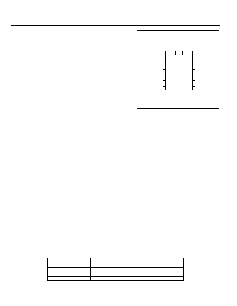
8-PIN DIP
SOIC
T
A
AVAILABLE OPTIONS
QProxTM
TM
TM
TM QT110 / QT110H
C
HARGE
-T
RANSFER
T
OUCH
S
ENSOR
Sns2
Vss
Sns1
Gain
Opt2
Opt1
Out
Vdd
1
2
3
4
5
6
7
8
Q
T
110
1 - OVERVIEW
The QT110 is a digital burst mode charge-transfer (QT)
sensor designed specifically for touch controls; it includes all
hardware and signal processing functions necessary to
provide stable sensing under a wide variety of changing
conditions. Only a single low cost, non-critical capacitor is
required for operation.
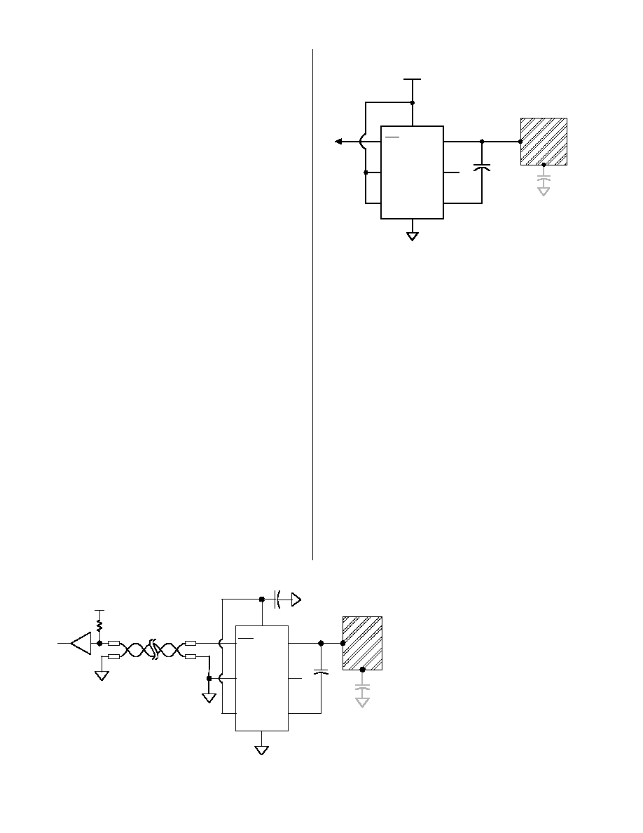
Figure 1-1 shows the basic QT110 circuit using the device,
with a conventional output drive and power supply
connections. Figure 1-2 shows a second configuration using
a common power/signal rail which can be a long twisted pair
from a controller; this configuration uses the built-in pulse
mode to transmit output state to the host controller (QT110
only).
1.1 BASIC OPERATION
The QT110 employs short, ultra-low duty cycle bursts of
charge-transfer cycles to acquire its signal. Burst mode
permits power consumption in the low microamp range,
dramatically reduces RF emissions, lowers susceptibility to
EMI, and yet permits excellent response time. Internally the
signals are digitally processed to reject impulse noise, using
a 'consensus' filter which requires four consecutive
confirmations of a detection before the output is activated.
The QT switches and charge measurement hardware
functions are all internal to the QT110 (Figure 1-3). A 14-bit
single-slope switched capacitor ADC includes both the
required QT charge and transfer switches in a configuration
that provides direct ADC conversion. The ADC is designed to
dynamically optimize the QT burst length according to the
rate of charge buildup on Cs, which in turn depends on the
values of Cs, Cx, and Vdd. Vdd is used as the charge
reference voltage. Larger values of Cx cause the charge
transferred into Cs to rise more rapidly, reducing available
resolution; as a minimum resolution is required for proper
operation, this can result in dramatically reduced apparent
gain. Conversely, larger values of Cs reduce the rise of
differential voltage across it, increasing available resolution
by permitting longer QT bursts. The value of Cs can thus be
increased to allow larger values of Cx to be tolerated
(Figures 4-1, 4-2, 4-3 in Specifications, rear).
The IC is highly tolerant of changes in Cs since it computes
the threshold level ratiometrically with respect to absolute
load, and does so dynamically at all times.
Cs is thus non-critical; as it drifts with temperature, the
threshold algorithm compensates for the drift automatically.
A simple circuit variation is to replace Cs with a bare piezo
sounder (Section 2), which is merely another type of
capacitor, albeit with a large thermal drift coefficient. If C
piezo
is in the proper range, no other external component is
required. If C
piezo
is too small, it can simply be `topped up'
with an inexpensive ceramic capacitor connected in parallel
with it. The QT110 drives a 4kHz signal across SNS1 and
SNS2 to make the piezo (if installed) sound a short tone for
75ms immediately after detection, to act as an audible
confirmation.
Option pins allow the selection or alteration of several
special features and sensitivity.
1.2 ELECTRODE DRIVE
The internal ADC treats Cs as a floating transfer capacitor;
as a direct result, the sense electrode can be connected to
either SNS1 or SNS2 with no performance difference. In both
cases the rule Cs >> Cx must be observed for proper
operation. The polarity of the charge buildup across Cs
during a burst is the same in either case.
It is possible to connect separate Cx and
Cx' loads to SNS1 and SNS2
simultaneously, although the result is no
different than if the loads were
connected together at SNS1 (or SNS2).
It is important to limit the amount of
stray capacitance on both terminals,
especially if the load Cx is already large,
for example by minimizing trace lengths
and widths so as not to exceed the Cx
load specification and to allow for a
larger sensing electrode size if so
desired.
The PCB traces, wiring, and any
components associated with or in
contact with SNS1 and SNS2 will
become touch sensitive and should be
- 2 -
Figure 1-1 Standard mode options
S E NS ING
E LEC TRO DE
C
s
1 0nF
3
4
6
5
1
+2.5 to 5
7
2
OU T
OP T1
OP T2
G A IN
S NS1
S NS2
Vss
Vdd
OU TP UT=D C
TIM EO UT= 10 S ecs
TOGG LE=OF F
GA IN= HIGH
C
x
8
Figure 1-2 2-wire operation, self-powered (QT110 only)
C
x
+
22 µF 10V AL
10 nF
C M O S
GATE
+3V
2.2k
Tw isted
pair
C
s
8
S E NS IN G
E LE C TRO DE
O UT
O PT1
O PT2
G A IN
S NS 1
S NS 2
V ss
V dd
3
4
6
5
1
7
2

treated with caution to limit the touch
area to the desired location. Multiple
touch electrodes can be used, for
example to create a control button on
both sides of an object, however it is
impossible for the sensor to distinguish
between the two touch areas.
1.3 ELECTRODE DESIGN
1.3.1 E
LECTRODE
G
EOMETRY
AND
S
IZE
There is no restriction on the shape of
the electrode; in most cases common
sense and a little experimentation can
result in a good electrode design. The
QT110 will operate equally well with
long, thin electrodes as with round or
square ones; even random shapes are
acceptable. The electrode can also be
a 3-dimensional surface or object.
Sensitivity is related to electrode
surface area, orientation with respect
to the object being sensed, object composition, and the
ground coupling quality of both the sensor circuit and the
sensed object.
If a relatively large electrode surface is desired, and if tests
show that the electrode has more capacitance than the
QT110 can tolerate, the electrode can be made into a sparse
mesh (Figure 1-4) having lower Cx than a solid plane.
Sensitivity may even remain the same, as the sensor will be
operating in a lower region of the gain curves.
1.3.2 K
IRCHOFF
'
S
C
URRENT
L
AW
Like all capacitance sensors, the QT110 relies on Kirchoff's
Current Law (Figure 1-5) to detect the change in capacitance
of the electrode. This law as applied to capacitive sensing
requires that the sensor's field current must complete a loop,
returning back to its source in order for capacitance to be
sensed. Although most designers relate to Kirchoff's law with
regard to hardwired circuits, it applies equally to capacitive
field flows. By implication it requires that the signal ground
and the target object must both be coupled together in some
manner for a capacitive sensor to operate properly. Note that
there is no need to provide actual hardwired ground
connections; capacitive coupling to ground (Cx1) is always
sufficient, even if the coupling might seem very tenuous. For
example, powering the sensor via an isolated transformer
will provide ample ground coupling, since there is
capacitance between the windings and/or the transformer
core, and from the power wiring itself directly to 'local earth'.
Even when battery powered, just the physical size of the
PCB and the object into which the electronics is embedded
will generally be enough to couple a few picofarads back to
local earth.
1.3.3 V
IRTUAL
C
APACITIVE
G
ROUNDS
When detecting human contact (e.g. a fingertip), grounding
of the person is never required. The human body naturally
has several hundred picofarads of `free space' capacitance
to the local environment (Cx3 in Figure 1-5), which is more
than two orders of magnitude greater than that required to
create a return path to the QT110 via earth. The QT110's
PCB however can be physically quite small, so there may be
little `free space' coupling (Cx1 in Figure 1-5) between it and
the environment to complete the return path. If the QT110
circuit ground cannot be earth grounded by wire, for example
via the supply connections, then a `virtual capacitive ground'
may be required to increase return coupling.
- 3 -
Figure 1-3 Internal Switching & Timing
C
s
C
x
SNS2
SNS1
ELE C TRO DE
S
i
ng
le
-
S
lo
p
e
1
4
-
b
i
t
S
w
i
t
c
h
e
d
C
a
p
a
c
i
to
r
A
D
C
Charge
Am p
Bu
rst
C
o
n
t
ro
l
l
e
r
Result
Do ne
Start
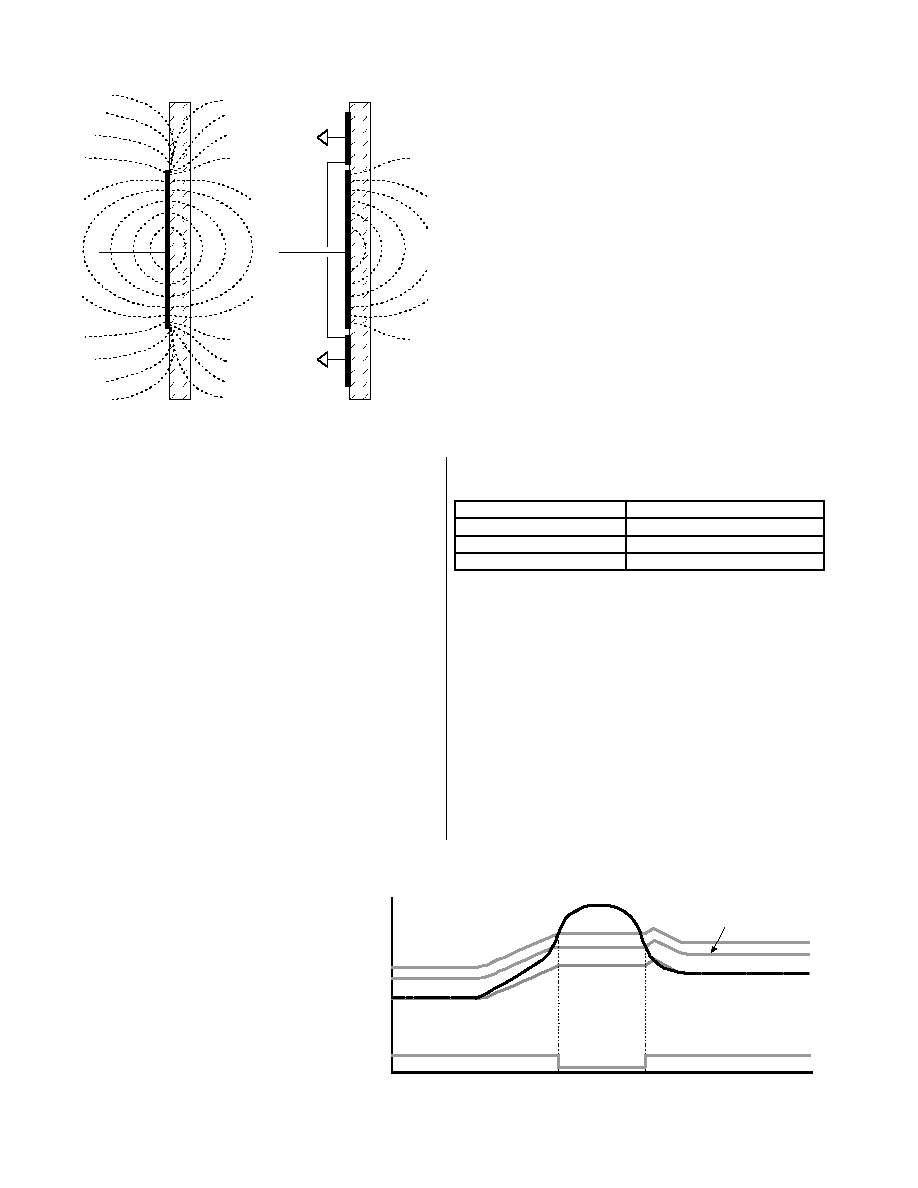
Figure 1-4 Mesh Electrode Geometry
Figure 1-5 Kirchoff's Current Law
S e n se E le ctro de
C
X2
Su rro und ing e nv iro nm ent
C
X3
S ENSO R
C
X1
A `virtual capacitive ground' can be created by connecting
the QT110's own circuit ground to:
(1) A nearby piece of metal or metallized housing;
(2) A floating conductive ground plane;
(3) A nail driven into a wall when used with small
electrodes;
(4) A larger electronic device (to which its output might be
connected anyway).
Free-floating ground planes such as metal foils should
maximize exposed surface area in a flat plane if possible. A
square of metal foil will have little effect if it is rolled up or
crumpled into a ball. Virtual ground planes are more
effective and can be made smaller if they are physically
bonded to other surfaces, for example a wall or floor.
1.3.4 F
IELD
S
HAPING
The electrode can be prevented from sensing in undesired
directions with the assistance of metal shielding connected
to circuit ground (Figure 1-6). For example, on flat surfaces,
the field can spread laterally and create a larger touch area
than desired. To stop field spreading, it is only necessary to
surround the touch electrode on all sides with a ring of metal
connected to circuit ground; the ring can be on the same or
opposite side from the electrode. The ring will kill
field spreading from that point outwards.
If one side of the panel to which the electrode is
fixed has moving traffic near it, these objects can
cause inadvertent detections. This is called
`walk-by' and is caused by the fact that the fields
radiate from either surface of the electrode
equally well. Again, shielding in the form of a
metal sheet or foil connected to circuit ground
will prevent walk-by; putting a small air gap
between the grounded shield and the electrode
will keep the value of Cx lower and is
encouraged. In the case of the QT110, the
sensitivity is low enough that 'walk-by' should not
be a concern if the product has more than a few
millimeters of internal air gap; if the product is very thin and
contact with the product's back is a concern, then some form
of rear shielding may be required.
1.3.5 S
ENSITIVITY
The QT110 can be set for one of 3 gain levels using option
pin 5 (Table 1-1). If left open, the gain setting is high. The
sensitivity change is made by altering the numerical
threshold level required for a detection. It is also a function
of other things: electrode size, shape, and orientation, the
composition and aspect of the object to be sensed, the
thickness and composition of any overlaying panel material,
and the degree of ground coupling of both sensor and object
are all influences.
1.3.5.1 Increasing Sensitivity
In some cases it may be desirable to increase sensitivity
further, for example when using the sensor with very thick
panels having a low dielectric constant.
Sensitivity can often be increased by using a bigger
electrode, reducing panel thickness, or altering panel
composition. Increasing electrode size can have diminishing
returns, as high values of Cx will reduce sensor gain
(Figures 4-1 ~ 4-3). Also, increasing the electrode's surface
area will not substantially increase touch sensitivity if its
diameter is already much larger in surface area than the
object being detected. The panel or other intervening
material can be made thinner, but again there are
diminishing rewards for doing so. Panel material can also be
changed to one having a higher dielectric constant, which
will help propagate the field through to the front. Locally
adding some conductive material to the panel (conductive
materials essentially have an infinite dielectric constant) will
also help dramatically; for example, adding carbon or metal
fibers to a plastic panel will greatly increase frontal field
strength, even if the fiber density is too low to make the
plastic bulk-conductive.
1.3.5.2 Decreasing Sensitivity
In some cases the QT110 may be too sensitive, even on low
gain. In this case gain can be lowered further by any of a
- 4 -
Figure 1-6
Shielding Against Fringe Fields
Sen se
wire
Sense
wire
U nshielded
Electrode
S hielded
E lectrode
Figure 2-1 Drift Compensation
T hr eshold
S ignal
H ysteresis
R eference
Output
Pin 7
Low
Pin 6
Medium
None
High
Tie Pin 5 to:
Gain
Table 1-1 Gain Setting Strap Options

number of strategies: making the electrode smaller,
connecting a very small capacitor in series with the sense
lead, or making the electrode into a sparse mesh using a
high space-to-conductor ratio (Figure 1-4). A deliberately
added Cx capacitor can also be used to reduce sensitivity
according to the gain curves (see Section 4).
Intermediate levels of gain (e.g. between 'medium' and 'low'
can be obtained by a combination of jumper settings with
one or more of the above strategies.
2 - QT110 SPECIFICS
2.1 SIGNAL PROCESSING
The QT110 processes all signals using 16 bit math, using a
number of algorithms pioneered by Quantum. The
algorithms are specifically designed to provide for high
'survivability' in the face of all kinds of adverse
environmental changes.
2.1.1 D
RIFT
C
OMPENSATION
A
LGORITHM
Signal drift can occur because of changes in Cx and Cs over
time. It is crucial that drift be compensated for, otherwise
false detections, non-detections, and sensitivity shifts will
follow.
Drift compensation (Figure 2-1) is performed by making the
reference level track the raw signal at a slow rate, but only
while there is no detection in effect. The rate of adjustment
must be performed slowly, otherwise legitimate detections
could be ignored. The QT110 drift compensates using a
slew-rate limited change to the reference level; the threshold
and hysteresis values are slaved to this reference.
Once an object is sensed, the drift compensation
mechanism ceases since the signal is legitimately high, and
therefore should not cause the reference level to change.
The QT110's drift compensation is 'asymmetric': the
reference level drift-compensates in one direction faster than
it does in the other. Specifically, it compensates faster for
decreasing signals than for increasing signals. Increasing
signals should not be compensated for quickly, since an
approaching finger could be compensated for partially or
entirely before even touching the sense pad. However, an
obstruction over the sense pad, for which the sensor has
already made full allowance for, could suddenly be removed
leaving the sensor with an artificially elevated reference level
and thus become insensitive to touch. In this latter case, the
sensor will compensate for the object's removal very quickly,
usually in only a few seconds.
2.1.2 T
HRESHOLD
C
ALCULATION
Sensitivity is dependent on the threshold level as well as
ADC gain; threshold in turn is based on the internal signal
reference level plus a small differential value. The threshold
value is established as a percentage of the absolute signal
level. Thus, sensitivity remains constant even if Cs is altered
dramatically, so long as electrode coupling to the user
remains constant. Furthermore, as Cx and Cs drift, the
threshold level is automatically recomputed in real time so
that it is never in error.
The QT110 employs a hysteresis dropout below the
threshold level of 50% of the delta between the reference
and threshold levels.
2.1.3 M
AX
O
N
-D
URATION
If an object or material obstructs the sense pad the signal
may rise enough to create a detection, preventing further
operation. To prevent this, the sensor includes a timer which
monitors detections. If a detection exceeds the timer setting,
the timer causes the sensor to perform a full recalibration.
This is known as the Max On-Duration feature.
After the Max On-Duration interval, the sensor will once
again function normally, even if partially or fully obstructed,
to the best of its ability given electrode conditions. There are
two timeout durations available via strap option: 10 and 60
seconds.
2.1.4 D
ETECTION
I
NTEGRATOR
It is desirable to suppress detections generated by electrical
noise or from quick brushes with an object. To accomplish
this, the QT110 incorporates a detect integration counter that
increments with each detection until a limit is reached, after
which the output is activated. If no detection is sensed prior
to the final count, the counter is reset immediately to zero.
In the QT110, the required count is 4.
The Detection Integrator can also be viewed as a
'consensus' filter, that requires four detections in four
successive bursts to create an output. As the basic burst
spacing is 75ms, if this spacing was maintained throughout
all 4 counts the sensor would react very slowly. In the
QT110, after an initial detection is sensed, the remaining
three bursts are spaced about 18ms apart, so that the
slowest reaction time possible is 75+18+18+18 or 129ms
and the fastest possible is 54ms, depending on where in the
initial burst interval the contact first occurred. The response
time will thus average 92ms.
- 5 -
10s
Vdd
Gnd
Pulse
10s
Gnd
Gnd
Toggle
60s
Gnd
Vdd
DC Out
10s
Vdd
Vdd
DC Out
Max On-
Duration
Tie
Pin 4 to:
Tie
Pin 3 to:
Table 2-1 Output Mode Strap Options
Figure 2-2 Powering From a CMOS Port Pin
0 . 0 1 µF
C MO S
m icro controller
O U T
P O RT X .m
P O RT X .n
V d d
V ss
Q T110