 | –≠–ª–µ–∫—Ç—Ä–æ–Ω–Ω—ã–π –∫–æ–º–ø–æ–Ω–µ–Ω—Ç: QT320-IS | –°–∫–∞—á–∞—Ç—å:  PDF PDF  ZIP ZIP |

L
Q
QP
ROX
TM
QT320
2-C
HANNEL
P
ROGAMMABLE
A
DVANCED
S
ENSOR
IC
Two channel digital advanced capacitive sensor IC
Projects two `touch buttons' through any dielectric
Cloning for user-defined sensing behavior
100% autocal - no adjustments required
Only one external capacitor per channel
User-defined drift compensation, threshold levels
Variable gain via Cs capacitor change
Selectable output polarities
Toggle mode / normal mode outputs
HeartBeatTM health indicator on outputs (can be disabled)
1.8 ~ 5V supply, 60µA
APPLICATIONS
Computer peripherals
Entertainment devices
Access systems
Pointing devices
Appliance control
Security systems
Light switches
Industrial panels
The QT320 charge-transfer ("QT'") touch sensor chip is a self-contained digital IC capable of detecting near-proximity or
touch on two sensing channels. It will project sense fields through almost any dielectric, like glass, plastic, stone, ceramic,
and most kinds of wood. It can also turn small metal-bearing objects into intrinsic sensors, making them respond to proximity
or touch. This capability coupled with its ability to self calibrate continuously can lead to entirely new product concepts.
It is designed specifically for human interfaces, like control panels, appliances, security systems, lighting controls, or
anywhere a mechanical switch or button may be found; it may also be used for some material sensing and control
applications provided that the presence duration of objects does not exceed the recalibration time-out interval.
The IC requires only a common inexpensive capacitor per channel in order to function.
Power consumption and speed can be traded off depending on the application; drain can be as low as 60
µA, allowing
operation from batteries.
The IC's RISC core employs signal processing techniques pioneered by Quantum; these are specifically designed to make
the device survive real-world challenges, such as `stuck sensor' conditions and signal drift. Even sensitivity is digitally
determined. All key operating parameters can be set by the designer via the onboard eeprom which can be configured to alter
sensitivity, drift compensation rate, max on-duration, output polarity, and toggle mode independently on each channel.
No external switches, opamps, or other analog components aside from Cs are usually required.
The Quantum-pioneered HeartBeatTM signal is also included, allowing a host controller to monitor the health of the QT320
continuously if desired; this feature can be disabled via the cloning process.
By using the charge transfer principle, the IC delivers a level of performance clearly superior to older technologies in a highly
cost-effective package.
L
Q
Copyright © 2002 QRG Ltd
QT320/R1.03 08/02
-
QT320-IS
-40
0
C to +85
0
C
QT320-D
-
0
0
C to +70
0
C
8-PIN DIP
SOIC
T
A
AVAILABLE OPTIONS
Serial clone data in
SDI
7
Serial clone data out
SDO
6
Serial clone data clock
SCK
3
Alternate Pin Functions for Cloning
Positive supply
VDD
8
Detection output, Ch. 2
OUT2
7
Sense Ch 2 pin A
S2A
6
Sense Ch 1 pin B
S1B
5
Negative supply (ground)
VSS
4
Sense Ch 1 pin A
S1A
3
Sense Ch 2 pin B
S2B
2
Detection output, Ch. 1
OUT1
1
Function
Name
Pin
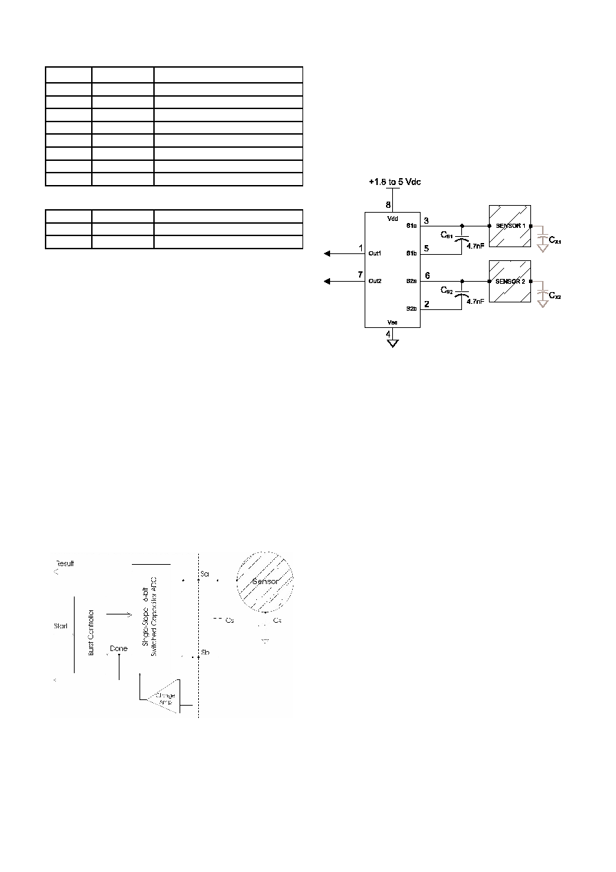
Table 1-1 Pin Descriptions
1 - OVERVIEW
The QT320 is a 2 channel digital burst mode charge-transfer
(QT) sensor designed specifically for touch controls; it
includes all hardware and signal processing functions
necessary to provide stable sensing under a wide variety of
changing conditions. Only two low-cost, non-critical capacitors
are required for operation.
A unique aspect of the QT320 is the ability of the designer to
`clone' a wide range of user-defined setups into the part's
eeprom during development and in production. Cloned setups
can dramatically alter the behavior of each channel,
independently. For production, the parts can be cloned
in-circuit or can be procured from Quantum pre-cloned.
Figure 1-1 shows the basic QT320 circuit using the device,
with a conventional output drive and power supply
connections.
1.1 BASIC OPERATION
The QT320 employs bursts of variable-length charge-transfer
cycles to acquire its signal. Burst mode permits power
consumption in the microamp range, dramatically reduces RF
emissions, lowers susceptibility to EMI, and yet permits
excellent response time. Internally the signals are digitally
processed to reject impulse noise using a 'consensus' filter
which requires several consecutive confirmations of a
detection before an output is activated.
The two channels of sensing operate in a completely
independent fashion. A unique cloning process allows the
internal eeprom of the device to be programmed for each
channel, to permit unique combinations of sensing and
processing functions for each.
The two sensing channels operate in interleaved
time-sequence and thus cannot interfere with each other.
1.2 ELECTRODE DRIVE
1.2.1 S
WITCHING
O
PERATION
The IC implements two channels of direct-to-digital
capacitance acquisition using the charge-transfer method, in
a process that is better understood as a capacitance-
to-digital converter (CDC). The QT switches and charge
measurement functions are all internal to the IC (Figure 1-2).
The CDC treats sampling capacitor Cs as a floating store of
accumulated charge which is switched between the sense
pins; as a result, the sense electrode can be connected to
either pin with no performance difference. In both cases the
rule Cs >> Cx must be observed for proper operation. The
polarity of the charge build-up across Cs during a burst is the
same in either case. Typical values of Cs range from 2nF to
100nF for touch operation.
Larger values of Cx cause charge to be transferred into Cs
more rapidly, reducing available resolution and resulting in
lower gain. Conversely, larger values of Cs reduce the rise of
differential voltage across it, increasing available resolution
and raising gain. The value of Cs can thus be increased to
allow larger values of Cx to be tolerated (Figures 5-1 to 5-4).
As Cx increases, the length of the burst decreases resulting in
lower signal numbers.
It is possible to connect separate Cx and Cx' loads to Sa and
Sb simultaneously, although the result is no different than if
the loads were connected together at Sa (or Sb). It is
important to limit the amount of stray Cx capacitance on both
terminals, especially if the load Cx is already large. This can
be accomplished by minimising trace lengths and widths.
l
Q
2
QT320/R1.03 08/02
Figure 1-2 Internal Switching
Figure 1-1 Basic QT320 circuit

1.2.2 C
ONNECTION
TO
E
LECTRODES
The PCB traces, wiring, and any components associated with
or in contact with Sa and Sb of either channel will become
touch sensitive and should be treated with caution to limit the
touch area to the desired location.
Multiple touch electrodes can be connected to one sensing
channel, for example to create a control button on both sides
of an object, however it is impossible for the sensor to
distinguish between the two connected touch areas.
1.2.3 B
URST
M
ODE
O
PERATION
The acquisition process occurs in bursts (Figure 1-7) of
variable length, in accordance with the single-slope CDC
method. The burst length depends on the values of Cs and
Cx. Longer burst lengths result in higher gains and more
sensitivity for a given threshold setting, but consume more
average power and are slower.
Burst mode operation acts to lower average power while
providing a great deal of signal averaging inherent in the CDC
process, making the signal acquisition process more robust.
The QT method is a very low impedance method of sensing
as it loads Cx directly into a very large capacitor (Cs). This
results in very low levels of RF susceptibility.
1.3 ELECTRODE DESIGN
1.3.1 E
LECTRODE
G
EOMETRY
AND
S
IZE
There is no restriction on the shape of the electrodes; in most
cases common sense and a little experimentation can result
in a good electrode design. The QT320 will operate equally
well with long, thin electrodes as with round or square ones;
even random shapes are acceptable. The electrode can also
be a 3-dimensional surface or object. Sensitivity is related to
electrode surface area, orientation with respect to the object
being sensed, object composition, and the ground coupling
quality of both the sensor circuit and the sensed object.
Smaller electrodes will have less sensitivity than large ones.
If a relatively large electrode surfaces are desired, and if tests
show that an electrode has a high Cx capacitance that
reduces the sensitivity or prevents proper operation, the
electrode can be made into a mesh (Figure 1-3) which will
have a lower Cx than a solid electrode area.
1.3.2 K
IRCHOFF
'
S
C
URRENT
L
AW
Like all capacitance sensors, the QT320 relies on Kirchoff's
Current Law (Figure 1-4) to detect the change in capacitance
of the electrode. This law as applied to capacitive sensing
requires that the sensor's field current must complete a loop,
returning back to its source in order for capacitance to be
sensed. Although most designers relate to Kirchoff's law with
regard to hardwired circuits, it applies equally to capacitive
field flows. By implication it requires that the signal ground
and the target object must both be coupled together in some
manner in order for the sensor to operate properly. Note that
there is no need to provide an actual hardwired ground
connection; capacitive coupling to ground (Cx1) often is
sufficient, even if the coupling might seem very tenuous. For
example, powering the sensor via an isolated transformer will
almost always provide ample ground coupling, since there is
plenty of capacitance between the primary and secondary
windings via the transformer core and from there to the power
wiring itself directly to 'local earth'. Even when battery
powered, just the physical size of the PCB and the object into
which the electronics is embedded is often enough to couple
enough back to local earth.
The implications of Kirchoff's law can be most visibly
demonstrated by observing the E3B eval board's sensitivity
change between laying the board on a table versus holding
the board in your hand by it's batteries. The effect can also be
observed by holding the board only by one electrode, letting it
recalibrate, then touching the battery end; the board will work
quite well in this mode.
1.3.3 V
IRTUAL
C
APACITIVE
G
ROUNDS
When detecting human contact (e.g. a fingertip), grounding of
the person is never required, nor is it necessary to touch an
exposed metal electrode. The human body naturally has
several hundred picofarads of `free space' capacitance to the
local environment (Cx3 in Figure 1-4), which is more than two
orders of magnitude greater than that required to create a
return path to the QT320 via earth. The QT320's PCB
however can be physically quite small, so there may be little
`free space' coupling (Cx1 in Figure 1-4) between it and the
environment to complete the return path. If the QT320 circuit
ground cannot be grounded via the supply connections, then
l
Q
3
QT320/R1.03 08/02
Figure 1-4 Kirchoff's Current Law
Figure 1-3 Mesh Electrode Geometry
a `virtual capacitive ground' may be required to increase
return coupling.
A `virtual capacitive ground' can be created by connecting the
QT320's own circuit ground to:
(1) A nearby piece of metal or metallized housing;
(2) A floating conductive ground plane;
(3) A fastener to a supporting structure;
(4) A larger electronic device (to which its output might be
connected anyway).
Because the QT320 operates at a relatively low frequency,
about 500kHz, even long inductive wiring back to ground will
usually work fine.
Free-floating ground planes such as metal foils should
maximise exposed surface area in a flat plane if possible. A
square of metal foil will have little effect if it is rolled up or
crumpled into a ball. Virtual ground planes are more effective
and can be made smaller if they are physically bonded to
other surfaces, for example a wall or floor.
1.3.4 F
IELD
S
HIELDING
AND
S
HAPING
The electrode can be prevented from sensing in undesired
directions with the assistance of metal shielding connected to
circuit ground (Figure 1-5). For example, on flat surfaces, the
field can spread laterally and create a larger touch area than
desired. To stop field spreading, it is only necessary to
surround the touch electrode on all sides with a ring of metal
connected to circuit ground; the ring can be on the same or
opposite side from the electrode. The ring will kill field
spreading from that point outwards.
If one side of the panel to which the electrode is fixed has
moving traffic near it, these objects can cause inadvertent
detections. This is called `walk-by' and is caused by the fact
that the fields radiate from either surface of the electrode
equally well. Again, shielding in the form of a metal sheet or
foil connected to circuit ground will prevent walk-by; putting a
small air gap between the grounded shield and the electrode
will keep the value of Cx lower and is encouraged. In the case
of the QT320, sensitivity can be high enough (depending on
Cx and Cs) that 'walk-by' signals are a concern; if this is a
problem, then some form of rear shielding may be required.
1.4 SENSITIVITY ADJUSTMENTS
There are three variables which influence sensitivity
independently for each channel:
1. Cs (sampling capacitor)
2. Cx (unknown capacitance)
3. Signal threshold value
There is also a sensitivity dependence of the whole device on
Vdd. Cs and Cx effects are covered in Section 1.2.1.
The threshold setting can be adjusted independently for each
channel from 1 to 16 counts of signal swing (Section 2.2).
Note that sensitivity is also a function of other things like
electrode size, shape, and orientation, the composition and
aspect of the object to be sensed, the thickness and
composition of any overlaying panel material, and the degree
of mutual coupling of the sensor circuit and the object (usually
via the local environment, or an actual galvanic connection).
It is advisable to set the sensitivity to the approximate desired
result by changing Cx and Cs first using a signal threshold
fixed at 10. Use the threshold value thereafter to fine-tune
sensitivity.
1.4.1 I
NCREASING
S
ENSITIVITY
In some cases it may be desirable to greatly increase
sensitivity, for example when using the sensor with very thick
panels having a low dielectric constant, or when sensing low
capacitance objects.
Sensitivity can be increased by using a bigger electrode,
reducing panel thickness, or altering panel composition.
Increasing electrode size can have diminishing returns, as
high values of Cx load will also reduce sensor gain (Figures
5-1 to 5-4). The value of Cs also has a dramatic effect on
sensitivity, and this can be increased in value up to a limit.
Increasing electrode surface area will not substantially
increase sensitivity if its area is already larger than the object
to be detected. The panel or other intervening material can be
made thinner, but again there are diminishing rewards for
doing so. Panel material can also be changed to one having a
higher dielectric constant, which will help propagate the field.
Locally adding some conductive material to the panel
(conductive materials essentially have an infinite dielectric
constant) will also help; for example, adding carbon or metal
fibers to a plastic panel will greatly increase frontal field
l
Q
4
QT320/R1.03 08/02
Figure 1-5 Field Shielding & Shaping
Sense
wire
Sense
wire
Unshielded
Electrode
Shielded
Electrode
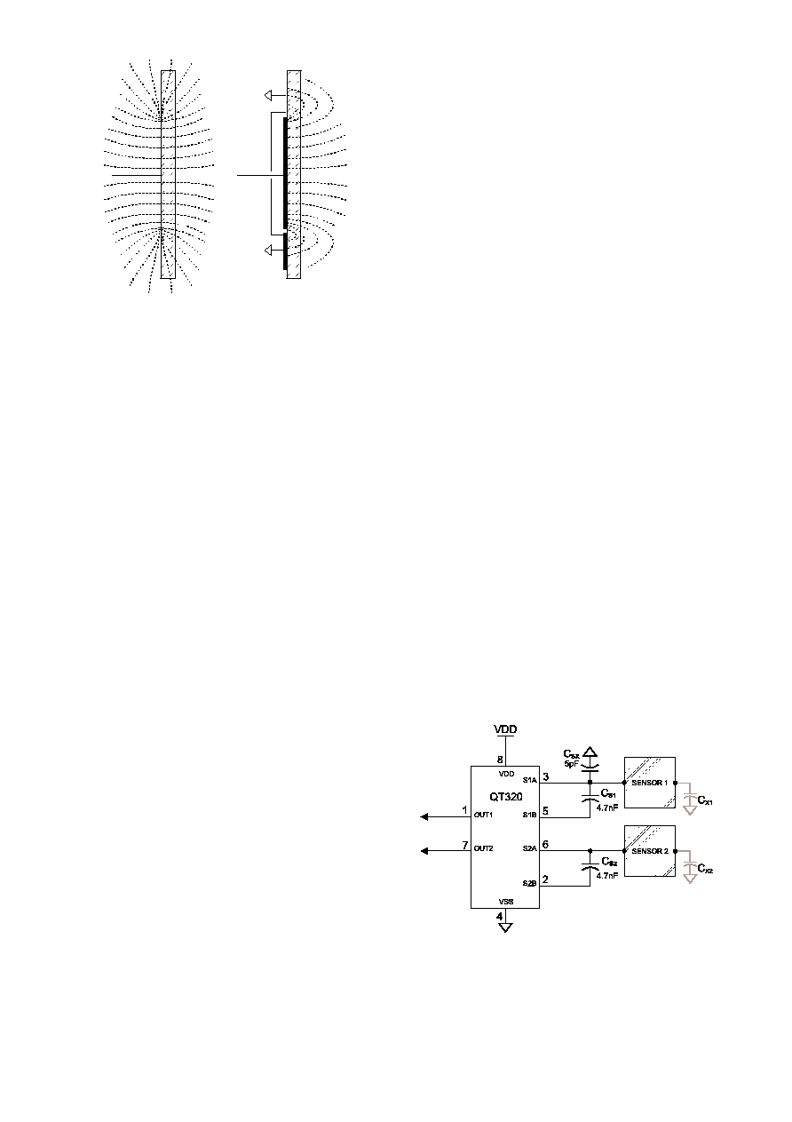
Figure 1-6 Circuit with Csx gain equalization capacitor
strength, even if the fiber density is too low to make the
plastic electrically conductive.
1.4.2 D
ECREASING
S
ENSITIVITY
In some cases the circuit may be too sensitive, even with high
signal threshold values. In this case gain can be lowered by
making the electrode smaller, using sparse mesh with a high
space-to-conductor ratio (Figure 1-3), and most importantly by
decreasing Cs. Adding Cx capacitance will also decrease
sensitivity.
It is also possible to reduce sensitivity by making a capacitive
divider with Cx by adding a low-value capacitor in series with
the electrode wire.
1.4.3 H
YSTERESIS
Hysteresis is required to prevent chattering of the output lines
with weak, noisy, or slow-moving signals.
The hysteresis can be set independently per channel.
Hysteresis is a reference-based number; thus, a threshold of
10 with a hysteresis of 2 will yield 2 counts of hysteresis
(20%); the channel will become active when the signal equals
or exceeds a count of 10, and go inactive when the count falls
to 7 or lower.
Hysteresis can also be set to zero (0), in which case the
sensor will go inactive when the count falls to 9 or lower in the
above example.
Threshold levels of under 4 counts are hard to deal with as
the hysteresis level is difficult to set properly.
1.4.4 C
HANNEL
B
ALANCE
Channel 1 has less internal Cx than Channel 2, which makes
it more sensitive than Channel 2 given equal Cx loads and Cs
capacitors. This can be useful in some designs where one
more sensitive channel is desired, but if equal sensitivity is
required a few basic rules should be followed:
1. Use a symmetrical PCB layout for both channels: Place
the IC half way between the two electrodes to match Cx
loading. Avoid routing ground plane (or other traces) close
to either sense line or the electrodes; allow 4-5 mm
clearance from any ground or other signal line to the
electrodes or their wiring. Where ground plane is required
(for example, under and around the QT320 itself) the
sense wires should have minimized adjacency to ground.
2. Connect a small capacitor (~5pF) between S1a or S1b
(either Channel 1 pin) and circuit ground (Csx in Figure
1-6), this will increase the load capacitance of Channel 1,
thus balancing the sensitivity of the two channels (see
Figures 1-7, 1-8).
3. Adjust Cs and/or the internal threshold of the two channels
until the sensitivities of the two channels are
indistinguishable from each other.
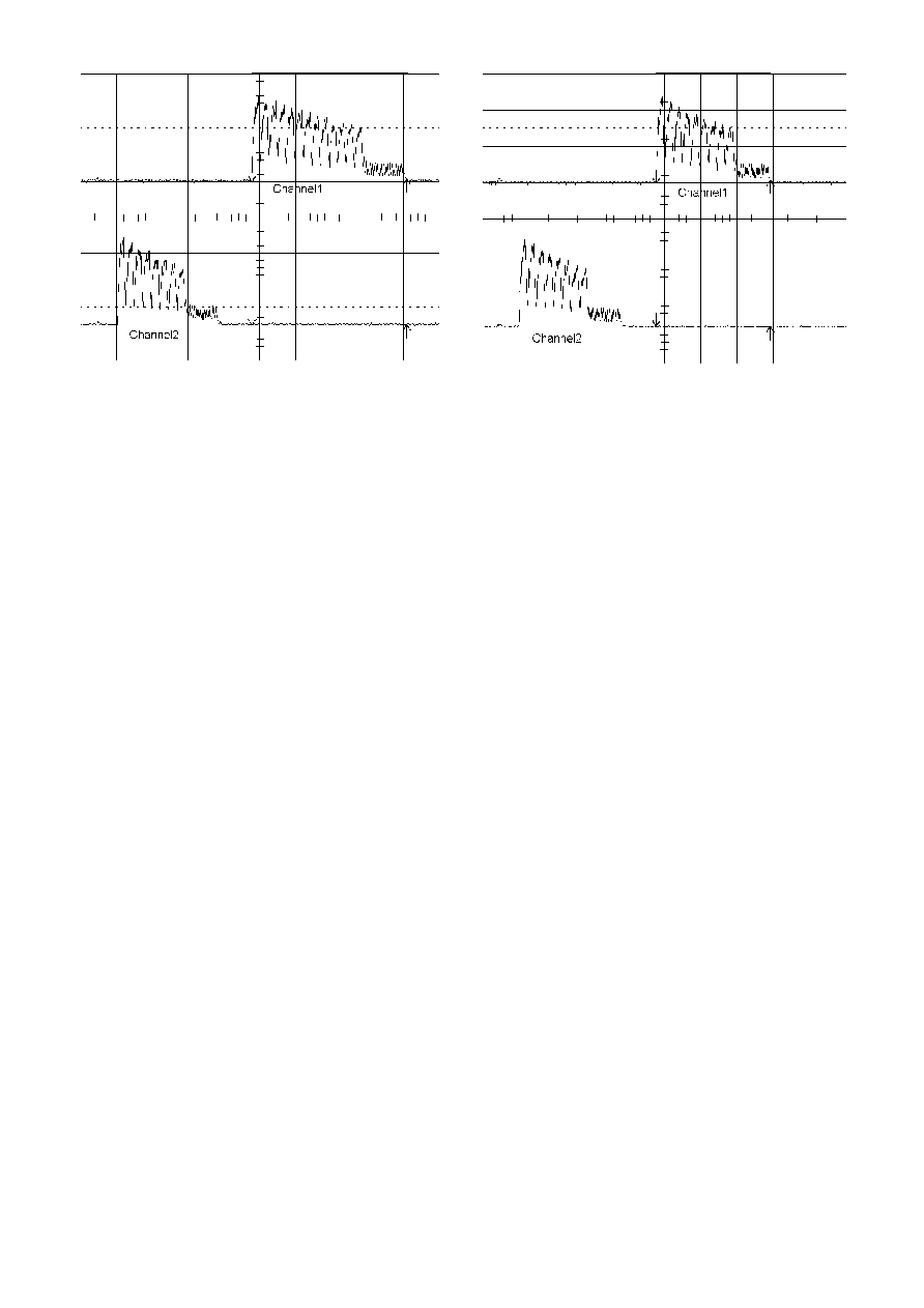
Since the actual burst length is proportional to sensitivity, you
can use an oscilloscope to balance the two channels with
more accuracy than by empirical methods (See Figures 1-7
and 1-8). Connect one scope probe to Channel 1 and the
other to Channel 2, via large resistors (750K ohms) to avoid
disturbing the measurement too much, or, use a low-C FET
probe. The Csx balance capacitor should be adjusted so that
the burst lengths of Channels 1 and 2 look nearly the same.
With some diligence the PCB can also be designed to include
some ground plane nearer to Channel 1 traces to induce
about 5pF of Csx load without requiring an actual discrete
capacitor.
l
Q
5
QT320/R1.03 08/02
Figure 1-8 Burst lengths with Csx installed
(observed using a 750K resistor in series with probe)
Figure 1-7 Burst lengths without Csx installed
(observed using a 750K resistor in series with probe)