4/ 4XLFN3&, 'DWD 6KHHW 5HY '
W
W
W
W
W
W
W W W W W W
4/ 4XLFN3&, 'DWD 6KHHW
0+]ELW 3&, 0DVWHU7DUJHW ZLWK (PEHGGHG 3URJUDPPDEOH
/RJLF DQG GXDO 3RUW 65$0
'HYLFH +LJKOLJKWV
+LJK 3HUIRUPDQFH 3&, &RQWUROOHU
64-bit / 66 MHz Master/Target PCI
Controller (automatically backwards
compatible to 33 MHz or/and 32-bits)
75 MHz PCI Interface supported for
embedded systems
PCI Specification v2.2 compliance
Programmable back-end interface with three
64-bit busses/100 MHz
Provides full 533 MB/s PCI data transfer
rates (600 MB/s at 75 MHz)
$GYDQFHG 3&, )HDWXUHV
DMA Chaining mode for queued DMA
transactions
Four-channel DMA mastering, plus a SPCI
(Single PCI Access) mode
Unlimited bursts supported in Master and
Target mode
Two Master Write FIFOs and two Master
Read FIFOs, each 64-deep and 64 bits wide
Target Read and Write FIFOs for pre-fetched
reads and multipleposted writes
Programmable interrupt controller
I2O compliant under microprocessor control
16 Mailbox registers for message passing and
semaphores
Extended configuration space allowing
Messaged Interrupts,
power management, and future PCI
enhancement support
([WUHPHO\ )OH[LEOH DQG &RQILJXUDEOH
Supports processor-less systems, as well as 0
wait-state burst connections to all known
8/16/32/64 bit processors
Includes non-volatile on-chip configuration
data for total customization
Independent PCI bus (66 MHz) and local bus
(100 MHz) clocks
All local interface, control, and glue-logic can
be implemented on chip
"PCI friendly" pinout simplifies board layout,
supports 4-layer PCI boards
$GYDQFHG 0DVWHU '0$ )HDWXUHV
Programmable DMA Channel Arbitration
Scheme
SPCI (Single PCI Access) mode may initiate
any PCI Master command
DMA controller configurable via PCI or
back-end
DMA Chaining mode allows a linked list of
DMA transfers to occur without user
intervention
+LJK 3HUIRUPDQFH 3&, 7DUJHW
Write posting FIFO increases performance
with queued transactions
(up to 16 queued writes)
Any BAR can be defined as pre-fetchable
Six base address registers supported,
configurable as memory or IO
Unique "Target Blast Mode" enables high-
performance and very low overhead
streaming data to/from PCI
ZZZTXLFNORJLFFRP
4XLFN/RJLF &RUSRUDWLRQ
W
W
W
W
W
W
4/ 4XLFN3&, 'DWD 6KHHW
([SDQGHG 3&, )XQFWLRQDOLW\
Support for Configuration Space from 0x40 to 0x3FF
PCI expanded capabilities support
Expansion ROM supported with back-end memory
Power management support
Compact PCI hot-swap/hot-plug compliant
Messaged Interrupts
Configuration specified with anti-fuses on board, external EEPROM not needed
3URJUDPPDEOH /RJLF
192 Programmable I/O pins in a 456 pin or 484 pin PBGA package
74K gates with 11 blocks (total of 12,672 bits) of dual-port RAM
250 MHz 16-bit counters, 275 MHz Datapaths, 160 MHz FIFOS
All back-end interface and glue-logic can be implemented
on chip
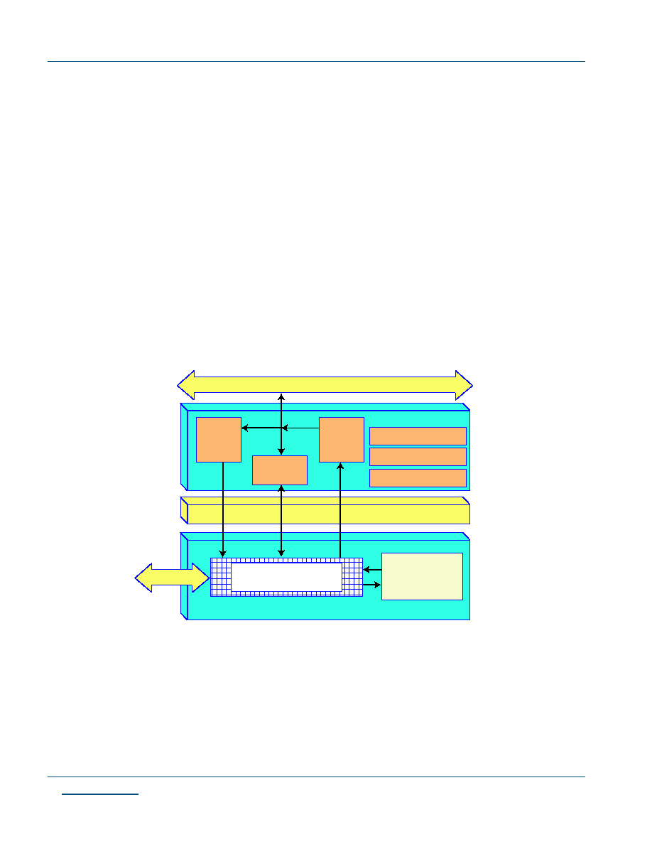
Figure 1: QL5064 Block Diagram
12k bits
Dual Port RAM
PROGRAMMABLE LOGIC
PCI CONTROLLER
100 MHz INTERFACE
64
64
64
3 RECV
FIFOs
64 deep
3 XMIT
FIFOs
64 deep
4 Channel
DMA Ctrl
Interrupts
Messaging
Config.
192 User I/O
PCI Bus - 33/66/75 MHz 32/64 Bits (Data and Address)
High Speed Logic Cells
74K Gates

4/ 4XLFN3&, 'DWD 6KHHW 5HY '
W
W
W
W
W
W
4/ 4XLFN3&, 'DWD 6KHHW
$UFKLWHFWXUH 2YHUYLHZ
The QL5064 device in the QuickLogic QuickPCI ESP (Embedded Standard Products) family provides a
complete and customizable PCI interface solution combined with 74,000 system gates of programmable
logic. This device eliminates any need for the designer to worry about PCI bus compliance, yet allows
for the maximum possible PCI bus bandwidth.
The programmable logic portion of the device is built from 792 QuickLogic Logic Cells, and 11
QuickLogic Dual-Port RAM Blocks. The configurable RAM blocks can each operate in 64x18, 128x9,
256x4, or 512x2 mode. These dual-port RAM blocks can be cascaded to achieve deeper or wider
configurations. They can also be combined with logic cells to form FIFOs. See the RAM section of this
data sheet for more information.
The QL5064 device includes a complete pre-designed PCI Initiator/Target interface offering full burst
mode transfers at 32 or 64 bits per clock cycle. At 66 MHz, this device offers support for 533
Mbytes/sec data transfer rates (66.6 MHz * 8 bytes per transfer). At the maximum speed of 75 MHz
(exceeding the current maximum speed specification for PCI), the QL5064 device can achieve 600
Mbytes/sec data transfer rates. The PCI interface is configured via internal programmable configuration
bits, so no external EEPROM or memory is needed.
The QL5064 device meets PCI 2.2 electrical and timing specifications and has been fully hardware-
tested. This device also supports the Win'98 and PC'98 standards. The QL5064 device features 3.3-
volt operation with multi-volt compatible I/Os. Thus it can easily operate in 3.3-volt only systems, as
well as mixed 3.3 volt/5 volt system. It can be placed on a universal signaling PCI board.
A wide range of additional features complements the QL5064 device. The FPGA side of the device is
5 volt and 3.3-volt PCI-compliant and is capable of implementing FIFOs at 160 MHz, and counters at
over 250 MHz. I/O pins provide individually controlled output enables, dedicated input/feedback
registers, and full JTAG capability for boundary scan and test. In addition, the QL5064 device provides
the benefits of non-volatility, high design security, immediate functionality on power-up, and a self-
contained single chip solution.

4/ 4XLFN3&, 'DWD 6KHHW 5HY '
W
W
W
W
W
W
4/ 4XLFN3&, 'DWD 6KHHW
$SSOLFDWLRQV
The QL5064 device supports maximum PCI transfer rates, so many applications exist which are ideally
suited to the device's high performance. High speed data communications, telecommunications, and
computing systems are just a few of the broad range of applications areas that can benefit from the high
speed PCI interface and programmable logic.
The PCI Interface can also act as a PCI Host Controller. This can be accomplished by glue-less interface
to most popular 8/16/32/64-bit microprocessors.
6L[ ),)2V IRU ,QFUHDVHG 3HUIRUPDQFH
The PCI interface includes the following
6 FIFO buffers:
2 64x64 PCI Master Transmit Buffers
2 64x64 PCI Master Receive Buffers
1 16x64 PCI Target Read/Pre-Fetch Buffer
1 32x64 PCI Target Write/Post Buffer
All FIFO buffers are 72 bits wide (64 data bits + 8-bit byte enables). PCI Initiator-mode buffers are 64
deep and support sustained burst transfers. PCI Target mode buffers are provided for both Read and
Write operations to the PCI Target, supporting pre-fetched reads with configurable registers.
All FIFOs can operate with independent read and write clocks, so that the programmable logic design
can interface to the FIFOs at up to 100 MHz (a clock asynchronous to the 33/66 MHz PCI clock). All
data synchronization is accomplished in the PCI core.
The transmit FIFOs have full flags and the receive FIFOs have empty flags. Both types of FIFOs have
programmable status flags that may be used to determine if either of the transmit FIFOs are almost full
or if either of the receive FIFOs are almost empty.