 | –≠–ª–µ–∫—Ç—Ä–æ–Ω–Ω—ã–π –∫–æ–º–ø–æ–Ω–µ–Ω—Ç: QL901M | –°–∫–∞—á–∞—Ç—å:  PDF PDF  ZIP ZIP |
© 2003 QuickLogic Corporation
www.quicklogic.com
∑
∑
∑
∑
∑
∑
Preliminary
1
∑ ∑ ∑ ∑ ∑ ∑
Device Highlights
CPU Core
∑ 32-bit MIPS 4Kc processor runs up to 133 MHz
(173 Dhrystone MIPS)
∑ 1.3 Dhrystone MIPS per MHz
∑ MDU supports MAC instructions for DSP
functions
∑ 16 KB of instruction cache (4-way set associative)
∑ 16 KB of data cache (4-way set associative),
lockable on a per line basis
SDRAM Memory Controller
∑ Support for PC-100 type SDRAMs, up to
256 MB total
∑ Two chip selects
∑ Operates at one-half CPU pipeline speed
∑ Support for x16 and x32 external memory bus
configurations
I/O Peripheral Controller
∑ Direct support for SRAM, EPROM and Flash
∑ 8-bit, 16-bit and 32-bit device widths supported
∑ Eight
independent chip selects
PCI Controller
∑ 32-bit v2.2 compatible
∑ Up to 66 MHz operation
∑ Supports host and satellite configurations
∑ Dedicated DMA channels for transmit and
receive bus transactions
∑ Support for external bus master arbitration
(through FPGA library provided by QuickLogic)
Two Ethernet Controllers
∑ Two 10/100 MACs
∑ Provides MII connection to external
transceivers/devices
Two UARTs
∑ One with modem control signals
∑ Both with IRDA-compliant signals
Four General Purpose 16-bit
Timer/Counters
∑ 16-bit prescaler to increase timer/counter delay
∑ Four modes of operation: decrement, increment,
interval, and Pulse Width Modulation (PWM)
∑ Operation from the System Bus clock or a clock
source supplied from the Programmable Fabric
System SRAM
∑ 16 KB accessible by all System Bus masters
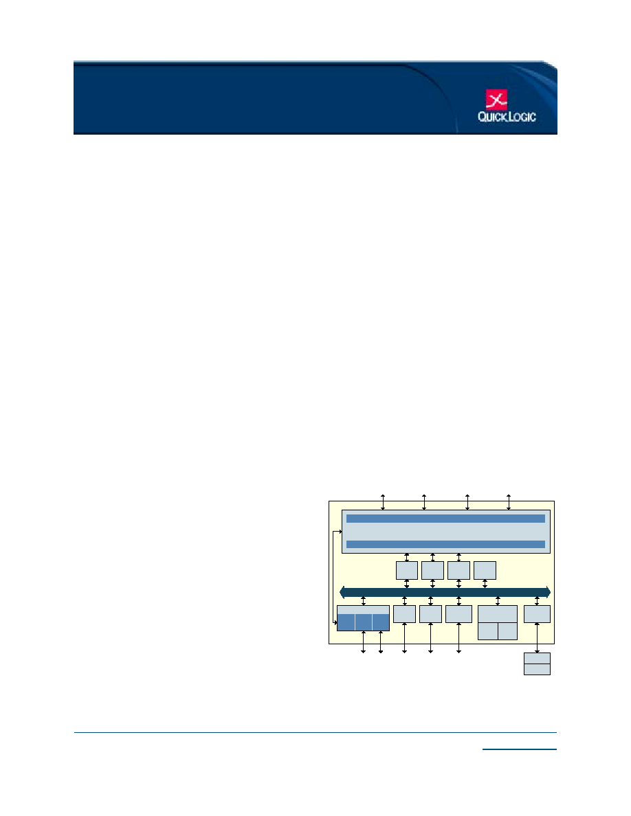
Figure 1: QL901M
Block Diagram
32 Bit System Bus (AMBA)
ViaLink FPGA
Fabric
Low Speed Peripherals
Memory
Controller
PCI
Controller
UART
(X2)
16 Bit
Timer
(X4)
ICU
SDRAM
32 Bit MIPS
4Kc
16K
SRAM
AHB
Master
APB
Slave (3)
16K
Dcache
16K
Icache
36 RAM Blocks (128x18, 256x9, 512x4, 1024x2)
18 ECU Blocks (8x8 Multiply, 16-bit carry/add)
AHB
Slave
10/100
Ethernet
10/100
Ethernet
MII
MII
SRAM
PCI 32/66
QuickMIPS Embedded Standard Product (ESP) Family
QL901M QuickMIPSTM Data Sheet

www.quicklogic.com
© 2003 QuickLogic Corporation
∑
∑
∑
∑
∑
∑
QL901M QuickMIPSTM Data Sheet Rev. D
Preliminary
2
High Performance 32-bit System Bus (AMBA Bus)
∑ Operates at one-half of CPU pipeline speed
∑ One 32-bit AHB master port/one 32-bit AHB slave port to programmable Fabric
∑ Three 32-bit APB slave ports in the programmable Fabric
Flexible Programmable Fabric
∑ 2016 logic cells (536 K system gates)
∑ 252 I/O pins
∑ 2.5 V Vcc, 2.5/3.3 V drive capable I/O
∑ 4,284 dedicated flip-flops
∑ IEEE 1149.1 boundary scan testing compliant
Dual-Port SRAM Modules
∑ Thirty-six 2,304 bit Dual-Port High Performance SRAM Blocks
∑ 82,944 embedded RAM bits
∑ RAM/ROM/FIFO Wizard for automatic configuration
∑ Configurable
and
cascadable
Programmable I/O
∑ High performance I/O cell with Tco <3 ns
∑ Programmable Slew Rate Control
∑ Programmable I/O Standards:
!
LVTTL, LVCMOS, PCI, GTL+, SSTL2, and SSTL3
!
Independent I/O Banks capable of supporting multiple standards in one device
!
I/O Register Configurations: Input, Output, Output Enable (OE)
Advanced Clock Network
∑ Multiple dedicated Low Skew Clock Networks
∑ High drive input-only networks
∑ Quadrant-based
segmentable clock networks
∑ Two User-programmable Phase Locked Loop (PLL) circuits
Embedded Computational Units (ECUs)
Eighteen hardwired DSP building blocks with integrated Multiply, Add, and Accumulate functions.

© 2003 QuickLogic Corporation
www.quicklogic.com
∑
∑
∑
∑
∑
∑
QL901M QuickMIPSTM Data Sheet Rev. D
Preliminary
3
Security Features
The QuickLogic products come with secure ViaLink
technology that protects intellectual property from
design theft and reverse engineering. No external configuration memory is needed for the Fabric. The device
is instant-on at power-up.
QuickWorks Design Software
The QuickWorks
package provides the most complete ESP and Field Programmable Gate Array (FPGA)
software solution from design entry to logic synthesis, to place and route, and simulation. The package
provides a solution for designers who use third party tools from Cadence, Mentor, Synopsys, and other third-
party tools for design entry, synthesis, or simulation.
Process Data
The QL901M is fabricated on a 0.25
µ
, six layer metal CMOS process. The core voltage is 2.5 V V
CC
supply
and the I/Os are up to 3.3 V tolerant. The QL901M is available in commercial and industrial temperature
grades.

www.quicklogic.com
© 2003 QuickLogic Corporation
∑
∑
∑
∑
∑
∑
QL901M QuickMIPSTM Data Sheet Rev. D
Preliminary
4
QL901M Architectural Overview
The QL901M chip can be thought of as having two distinct sides, an ASSP side and a Programmable Fabric
side. The ASSP side contains the standard cell circuitry of the device such as the MIPS 4Kc CPU and the
Ethernet MACs, and the Fabric side contains all of the programmable logic elements (e.g., logic cells and dual-
port RAMs) of the device.
ASSP Side
This section discusses the various circuits in the ASSP portion of the QL901M device.
CPU Core
The MIPS32 4Kc processor core is a high-performance, low-power, 32-bit MIPS RISC core capable of speeds
up to 233 MHz. The 4Kc core contains a fully-associative translation lookaside buffer (TLB) based Memory
Management Unit (MMU) and a pipelined MDU.
The core executes the MIPS32 instruction set architecture (ISA). It supports all application code in the MIPS I,
II, III, and IV instruction sets. It also supports kernel code for the R4000 processor and above. The MIPS32
ISA contains special multiply-accumulate, conditional move, prefetch, wait, and zero/one detect instructions.
The MMU contains a three-entry instruction TLB (ITLB), a three-entry data TLB (DTLB), and a 16 dual-entry
joint TLB (JTLB) with variable page sizes.
The 4Kc multiply-divide unit (MDU) supports a maximum issue rate of one 32x16 multiply
(MUL/MULT/MULTU), multiply-add (MADD/MADDU), or multiply-subtract (MSUB/MSUBU) operation per
clock, or one 32x32 MUL, MADD, or MSUB every other clock.
Instruction and Data Caches
The instruction and data caches are both 16 Kbytes in size. Each cache is organized as four-way set associative.
The data cache has lockout capability per cache line. On a cache miss, loads are blocked only until the first
critical word becomes available. The pipeline resumes execution while the remaining words are being written
to the cache. Both caches are virtually indexed and physically tagged. Virtual indexing allows the cache to be
indexed in the same clock in which the address is generated rather than waiting for the virtual-to physical
address translation in the MMU.
EJTAG Interface
The basic Enhanced JTAG (EJTAG) features provide CPU run control with stop, single stepping and re-start,
and software breakpoints through the SDBBP instruction. In addition, instruction and data virtual address
hardware breakpoints, and connection to an external EJTAG probe through the Test Access Port (TAP) is
included.

© 2003 QuickLogic Corporation
www.quicklogic.com
∑
∑
∑
∑
∑
∑
QL901M QuickMIPSTM Data Sheet Rev. D
Preliminary
5
ASSP PLL
On the ASSP side of the QL901M there is a single clock input that provides an input clock reference for the
MIPS core, the System Bus, and all ASSP peripherals (other than the PCI Controller, which is independently
driven by the PCI_CLK input). This clock input (PL_CLOCKIN) is the input to a PLL that is fixed at a two times
clock multiplication rate. For example, if the clock rate applied to PL_CLOCKIN is 50 MHz, the resultant clock
that drives the MIPS core is 100 MHz.
Table 1
shows the maximum input clock rates for PL_CLOCKIN based
upon the ASSP speed grade of the given QL901M device.
SDRAM Memory Controller
The QL901M SDRAM Memory Controller (SDMC) provides all the necessary logic to connect to a wide
variety of industry standard SDRAMs for use by the CPU, Ethernet Controllers and PCI bus and Ethernet
Controller. The SDMC supports a minimum SDRAM size of 16 Mbytes and a maximum SDRAM size of
256 Mbytes.
The SDRAM Controller controls the SDRAM on the external bus. On receiving an access request, the SDRAM
Controller decides on the appropriate commands to send to the SDRAM memory. The DRAM Bank
Controller sequences all of the commands required to complete a read or write request to an SDRAM memory
location with timing controlled by the CAS Delay and RAS Delay values.
The bus interface is a slave on the System Bus; it contains the control register block. The bus interface
produces read, write, refresh and mode register write requests to the SDRAM control engine, and software
supplied configuration information.
Data is transferred to and from the SDRAM as unbroken quad words. This data packet size is convenient for
cache line fills and buffered writes. For accesses smaller than a quad word, extra read data is ignored by the
SDRAM Controller; for writes, the SD_DQM(3:0) pins are used to force the SDRAMs to ignore invalid data.
For access sizes larger than a quad word, multiple quad word accesses are issued to the SDRAM control
engine.
I/O Peripheral Controller
This section describes access to I/O and memory devices on the external M Bus (with the exception of
SDRAM). The I/O Peripheral Controller (
Figure 2
) generates strobes and signals that can be used to interface
the M Bus with common asynchronous peripheral devices.
The QL901M Peripheral Controller Unit (PCU) provides decoded strobe signals to control external peripherals
such as SRAM, flash, real time clock (RTC) and memory mapped I/O devices. It supports 8-bit, 16-bit, and
32-bit widths with programmable wait states and bus turnaround time based on memory speed. The PCU
provides the following functionality:
∑ Decoding of memory access in the local CPUs memory map to generate chip selects or strobes.
∑ Control of wait states for decoded regions. A total of eight chip select signals are available. Chip select
seven is used as the boot ROM chip select.
Table 1: Maximum Input Frequency for PL_CLOCKIN and MIPS Core Frequency
Based on QL901M ASSP Speed Grade
QuickMIPS Device
Part Number Prefix
Maximum Input Frequency
for PL_CLOCKIN
Resultant Maximum
MIPS Core Frequency
QL901M-100
50 MHz
100 MHz
QL901M-133
66 MHz
133 MHz