Copyright © 1997, V3 Semiconductor Corp.
V96SSC Data Sheet Rev 2.3
1
V96SSC
Rev. B1
HIGH-INTEGRATION SYSTEM CONTROLLER
FOR i960
Æ
Sx/Jx AND PowerPC
TM
401Gx
PROCESSORS
V3 Semiconductor reserves the right to change the specifications of this product without notice.
V96SSC and V96xPBC are trademarks of V3 Semiconductor. All other trademarks are the property of their respective owners.
∑ Direct interface to i960Sx/Jx and PPC401Gx
processors
∑ High-performance burst DRAM controller
∑ Two-channel fly-by DMA controller
∑ Serial communications unit
∑ Programmable chip-select/strobe generation
∑ Support for 8/16-bit boot PROMs
∑ Two 32-bit general purpose timers
∑ Pulse width modulation capability
∑ System watchdog and heartbeat timers
∑ 16 general purpose I/O bits
∑ Eight input ports and eight output ports
∑ Interrupt control unit
∑ Local bus speeds up to 33MHz
∑ Low cost 100-pin EIAJ PQFP package
∑ Fastest time to market for i960Sx and i960Jx
based designs
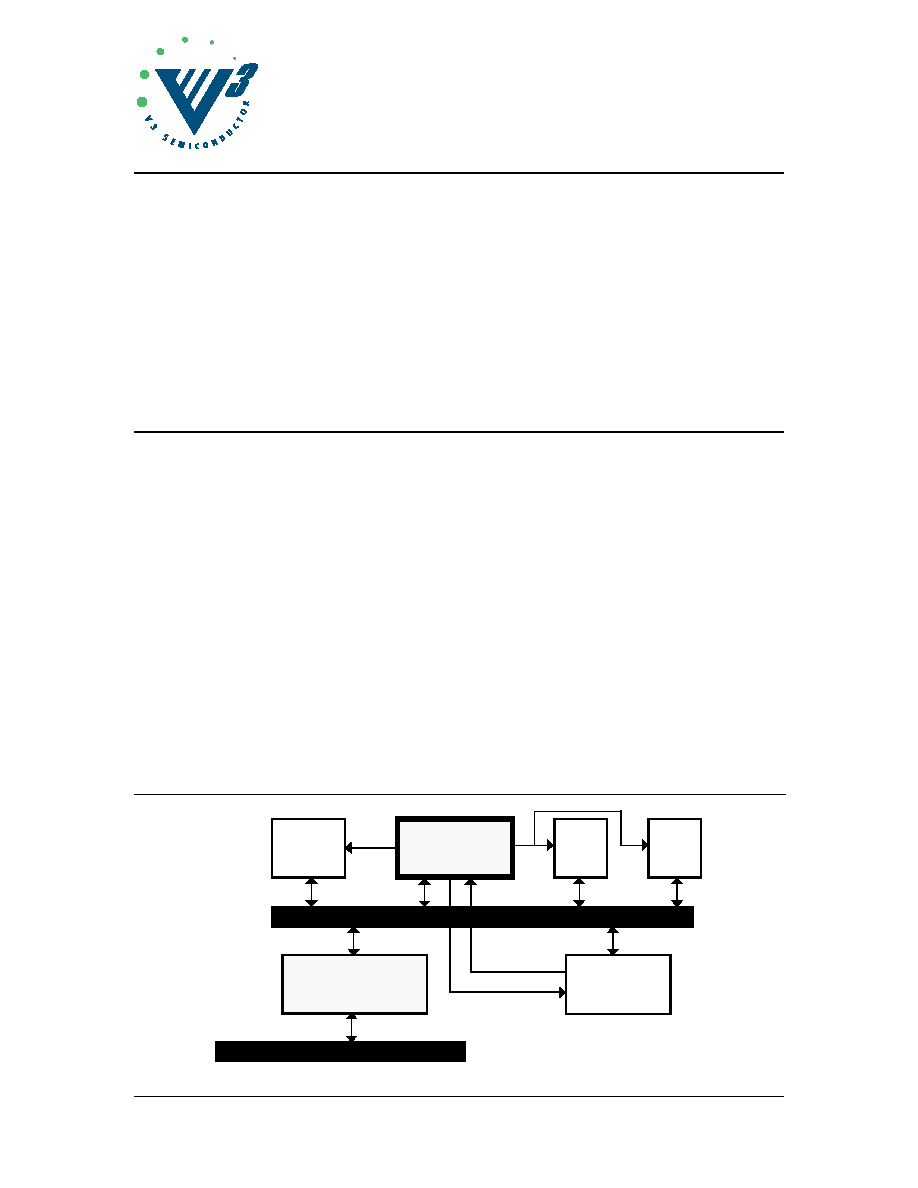
The V96SSC High-Integration System Controller
is a single-chip device that simplifies the design
o f s y s t e m s b a s e d o n i 9 6 0 S x , i 9 6 0 J x o r
PPC401Gx embedded microprocessors. The
V9 6S SC re place s ma ny lower integ ra tion
components with a single, high-integration
device.
Nearly all i960 or PowerPC processor based
systems will require DRAM for code and data
s t o r a g e . T h e V 9 6 S S C i n c l u d e s a h i g h -
p e r f o r m a n c e D R A M c o n t r o l l e r w h i c h i s
programmable to accommodate a wide range of
DRAM speeds and architectures.
The eight chip-select/strobes further simplify
peripheral/memory connection. Each select has
programmable timing and a total of four wait-
state generators are provided.
Beyond simplifying memory and peripheral
control, the V96SSC also includes many of the
peripherals needed to build a high-performance
i 9 6 0 o r P P C 4 0 1 G x b a s e d s y s t e m : D M A
channels, synchronous/asynchronous serial port,
general purpose and system heartbeat timers, bit
I/O ports, and an interrupt controller.
In a dd i tio n, th e V 96 SS C i nclu de s spe ci al
features to enhance system integrity. The bus
watch timer prevents system hangs on access to
unpopulated memory. A watchdog timer is also
included to recover from software upsets.
Due to its small footprint, and glueless interface,
the V96SSC provides the best features of an
integrated processor without any performance
compromises!
LOCAL BUS
LOCAL BUS
IRQs
DRAM
ARRAY
PROM
ADDR
CHIP SELECTS
AND STROBES
DMA REQUEST
LOCAL BUS
LOCAL BUS
PCI BUS
SYSTEM
CONTROLLER
V96SSC
DEVICE
NETWORKING
V960PBC or V961PBC
CONTROLLER
PCI BRIDGE
PPC401Gx
i960Sx/Jx
CPU
V96SSC
2
V96SSC Data Sheet Rev 2.3
Copyright © 1997, V3 Semiconductor Inc.
This document contains the product codes, pinouts, package mechanical information, DC
characteristics, and AC characteristics for the V96SSC. Detailed functional information is contained in
the User's Manual.
V3 Semiconductor retains the rights to change documentation, specifications, or device functionality at
any time without notice. Please verify that you have the latest copy of all documents before finalizing a
design.
1.0 Product Codes
2.0 Functional Description
The V96SSC consists of the following functional units:
∑ Direct i960 and PPC401Gx Processors Bus Interface Unit
∑ Burst DRAM Controller
∑ DMA Controller
∑ Serial Communications Unit
∑ Chip Select/Strobe Unit
∑ General Purpose Timer/Counters
∑ System Watchdog and System Heartbeat Timers
∑ Interrupt Control Unit
∑ I/O Control Unit and Internal Signal Multiplexer
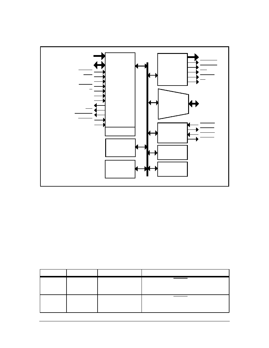
A block diagram of the V96SSC is shown in Figure 1. Each of the functional units is described briefly in
the sections below. The V96SSC Data Sheet provides information regarding AC and DC
specifications, pinout, and packaging. Detailed information regarding hardware and software
interfacing can be found in the V96SSC User's Manual
.
Table 1: Product Codes
Product Code
Processor
Bus Type
Package
Frequency
V96SSC-33LP
i960SA/SB
i960JA/JD/JF
PPC401GF
16-bit multiplexed
32-bit multiplexed
32-bit multiplexed
100-pin EIAJ PQFP
33MHz
V96SSC
Copyright © 1997, V3 Semiconductor Inc.
V96SSC Data Sheet Rev 2.3
3
Figure 1: V96SSC Block Diagram
2.1
Direct i960 Sx/Jx and PPC401Gx Processors Bus Interface Units
The V96SSC is designed to connect directly to i960Sx/Jx and PPC401Gx processors. No "glue logic"
is required. Care was taken during the design of the V96SSC to insure full AC timing compatibility with
these processors running with bus speeds up to 33MHz. Even the pinout of the V96SSC has been
designed with ease of connection in mind.
At the beginning of each processor bus cycle the V96SSC samples the BTYPE[1:0] pins. As it's shown
in the following table, these pins indicate what type of bus cycle is being run. Because the bus type is
dynamically detected, the V96SSC may be used in systems using both 16-bit and 32-bit masters.
Table 2: BTYPE[1:0] Pin Decoding
BTYPE[1:0]
CPU Mode
Boot Address
Description
00
i960SA/SB
A[31, 26:24]="0000"
16-bit data bus, BE[1:0] valid for current
cycle, both processor and V96SSC use 2x
clock
01
PPC401Gx
A[31, 26:24]="1111"
32-bit data bus, BE[3:0] valid for current
cycle, processor uses 1X clock and V96SSC
uses 2X clock
A31,A[26:16]
AD[15:0]
BE[1:0]
ADS
ALE
BLAST
W/R
BTYPE[1:0]
HLDA
HOLD
INT
RESOUT
RESET
CLK2
SYSTEM
HEARTBEAT/
WATCHDOG
TIMERS
BUS WATCH
i960
PROCESSOR
INTERFACE
SERIAL
COMM
UNIT
DRAM
CONTROL
MA[11:0]
RAS[1:0]
CAS[3:0]
WE
OE[1:0]
LE
I/O[15:0]
DREQ0
DACK0
DREQ1
DACK1
DMA
TWO
CHANNEL
CHIP SELECT
STROBE
LOGIC
32-BIT
TIMERS (2)
MUX
I/O
and
BIT I/O
V96SSC
4
V96SSC Data Sheet Rev 2.3
Copyright © 1997, V3 Semiconductor Inc.
In i960Sx systems, the low order address signals are latched internally from the AD[15:0] bus upon
assertion of ALE. The high-order address lines are demultiplexed on the i960Sx processor, and are
routed directly to the V96SSC's high order address inputs. The i960Jx processor uses a 32-bit
multiplexed address/data bus, therefore for i960Jx bus accesses, the V96SSC latches the high order
address signals internally on the assertion of ALE.
All accesses to V96SSC's internal registers are performed via the AD[15:0] lines. In 32-bit i960Jx
systems, the internal registers are typically accessed in a 32 bit region where access to the internal
registers is done by software 16 bits at a time (BTYPE="10"). Alternately, it can be mapped into a 16
bit region using BTYPE="11". While the V96SSC is internally a 16-bit device, it is capable of
supporting 32-bit memory and peripheral devices.
V96SSC also supports direct interface to PPC401Gx. When BTYPE="01" then the boot address
matches that of the PPC401Gx. In this mode a cycle can be initiated with either an ALE or ADS pulse.
Since the PPC401Gx has only an ALE output and lacks an ADS (AS) pin, ADS on the V96SSC can be
tied high by a pull-up resistor.
2.2
Burst DRAM Controller
The V96SSC's DRAM controller provides the following features:
∑ Support for fast page mode, extended data out, and Ramtron's enhanced DRAM architectures
∑ Two DRAM banks of up to 64MByte each (128MBytes total)
∑ Programmable DRAM bank address base and size
∑ Programmable row/column multiplexing mode
∑ Programmable RASx and CASx timings
∑ Support for 16-bit and 32-bit DRAM arrays
∑ Support for extended burst cycles up to 256 bytes transactions in length
∑ Programmable page caching to eliminate RAS cycles for subsequent accesses to the same
DRAM page
∑ Programmable refresh counter
∑ 1-0-0-0 read and 0-0-0-0 write performance at 33MHz
The burst DRAM controller is designed to support traditional fast page mode DRAMs (FPM), the new
extended data out page mode DRAMs (EDO), and Ramtron's ultra high-performance enhanced
DRAM (Ramtron EDRAM) devices. A wide variety of DRAM speeds and organizations may be
10
i960Jx
(32 bit bus)
A[31, 26:24]="1110"
32-bit data bus, BE[3:0] valid for current
cycle, processor uses 1X clock and V96SSC
uses 2X clock
11
i960Jx
(16 bit bus)
A[31, 26:24]="1110"
32-bit data bus, BE3 and BE0 valid for cur-
rent cycle, processor uses 1X clock and
V96SSC uses 2X clock
Table 2: BTYPE[1:0] Pin Decoding
BTYPE[1:0]
CPU Mode
Boot Address
Description

V96SSC
Copyright © 1997, V3 Semiconductor Inc.
V96SSC Data Sheet Rev 2.3
5
accommodated due to the V96SSC's flexibility.
Two DRAM banks are provided. Each bank has its own programmable address base and size. The
mapping of memory address lines to row and column addresses is also programmable for each bank.
The twelve mixed address lines (MA[11:0]) are shared by both banks. Each bank may be
independently enabled and/or write protected. Both banks share a common DRAM signal timing
generator that controls all DRAM timing parameters. DRAM array width can be set to either 16-bit or
32-bits; the V96SSC controls lane steering logic in mixed width systems.
FPM, EDO, and Ramtron EDRAMs are a natural fit for burst bus processors such as i960 or
PPC401Gx family. The V96SSC takes advantage of fast page mode accesses for every burst
transaction, insuring the highest transfer rate possible. The V96SSC also supports extended burst
peripherals, such as networking controllers, up to a maximum length of 64Byte data cycles.
The DRAM controller also includes page cache management logic. This logic detects subsequent
burst accesses within the same DRAM page, and eliminates the RAS precharge time and row address
cycles for these accesses. Removing these cycles can reduce the average wait-state profile for many
applications. The "aggressiveness" of the caching algorithm is programmable, and page caching can
be completely disabled. The page size is programmable from 512 to 8192 bytes.
2.3
DMA Controller
Two independent DMA Channels are provided in the V96SSC. The DMA Controller generates fly-by
cycles to transfer data directly from the DRAM to the selected peripheral, or vice-versa. Each channel
includes a request input (DREQx), an acknowledge output (DACKx), and an end-of-process output
(EOPx, accessible via the I/O Multiplexer). Each channel can also be assigned to a chip select/strobe
channel to provide the necessary strobing signals to the DMA target/source peripheral.
The DMA buffer start and stop addresses are programmable, as is the direction of transfer (read or
write). Transfers may be initiated either via the DREQx pins or through software.
The DMA Controller's programmable throttle count allows long transfers to be periodically interrupted
to allow the processor access to the bus for code fetches, etc.
2.4
Serial Communications Unit (SCU)
The V96SSC's Serial Communications Unit offers both synchronous and asynchronous modes. In
asynchronous mode, the Serial Communications Unit functions as an industry standard, full duplex
UART. Transmission and reception are double buffered to help prevent data overruns. Interrupts are
generated on receiver buffer full, transmit buffer empty, buffer overrun error, and framing error.
In synchronous (SPI) mode, data is moved into, or out of, the SCU's buffers on transitions of the serial
clock output pin (SCLK). Data word length is programmable from 1 to 16 bits. An interrupt is generated
upon completion of an SPI transfer. SPI mode is ideal for connecting to serial interface peripherals
such as A/D converters.
The clock reference for the Serial Communications Unit can be either the independent baud rate
generator or general purpose timer 1.
2.5
Chip Select/Strobe Unit
The Chip Select/Strobe Unit provides all the logic necessary to interface a wide array of peripherals
and memory components to the i960Sx/Jx processor. Address decoding, wait-state generation, chip-
select, and read/write strobe generation are handled completely by the V96SSC; no glue logic is