CLOCK
Page 1 of 3
R A L T R O N E L E C T R O N I C S C O R P .
!
1 0 6 5 1 N . W . 1 9
t h
S t
!
M i a m i , F l o r i d a 3 3 1 7 2
!
U . S . A .
phone: (305) 593-6033
!
fax: (305) 594-3973
!
e-mail: sales@raltron.com
!
WEB: http://www.raltron.com
CS9L/CSPL SERIES: ULTRA HF CLOCK OSCILLATOR, PECL, +3.3 VDC or +2.5VDC
DESCRIPTION: A crystal controlled, high frequency, highly stable oscillator, adhering to Positive Emitter
Coupled Logic (PECL) Standards and fundamental crystal or analog multiplication technologies. The output can
be Tri-stated to facilitate testing or combined multiple clocks. The device is contained in a sub-miniature, very low
profile, leadless ceramic SMD package with 6 gold contact pads. This miniature oscillator is ideal for today's
automated assembly environments.
APPLICATIONS AND FEATURES:
" Infiniband; Fiber Channel; SATA; 10GbE; Network Processors; SOHO Routing; Switches;
" Common Frequencies: 150 MHz; 156.25 MHz; 155.52 MHz; 161.1328 MHz; 212.5MHz; 312.5MHz
" +3.3 VDC or +2.5VDC PECL
" Frequency Range from 150.000 to 700 MHz
" Analog multiplication
" Miniature Ceramic SMD Package Available on Tape and Reel
" Lead Free and ROHS Compliant
$
$
$
$
ABSOLUTE MAXIMUM RATINGS:
PARAMETER
SYMBOL
VALUE
UNIT
Operating temperature range Ta
-40...+85
∞
C
Storage temperature range
T(stg)
-55...+90
∞
C
Supply voltage
Vcc
+4.6
VDC
Maximum Input Voltage
Vi
Vss-0.5...Vcc+0.5
VDC
Maximum Output Voltage
Vo
Vss-0.5...Vcc+0.5
VDC
$
$
$
$
ELECTRICAL PARAMETERS:
PARAMETER
SYMBO
L
TEST CONDITIONS
*1
VALUE
UNIT
Nominal Frequency
fo
150.000 ~ 700.00**
MHz
Supply Voltage
Vcc
+3.3 or +2.5
±
5%
VDC
Supply Current
Is
80.0 MAX
mA
Output Logic Type
PECL
Load
Connected between each output and Vcc ≠ 2.0 VDC
50
Output Voltage Levels
Voh
Vol
min
max
Vcc-1.025
Vcc-1.620
VDC
VDC
Duty Cycle
DC
Measured at 50% of Vcc
40/60 to 60/40 or 45/55 to 55/45
%
Rise / Fall Time
tr / tf
Measured at 20/80% and 80/20% Vcc Levels
0.7 TYP 1.0 MAX
*2
ns
Integrated Phase tji RMS, Fj = 12 kHz...20 MHz
5
0.3
TYP**
ps
Integrated Phase RMS tii offset frequency 50KHz to
80MHz
5
0.5 TYP**
ps
Fo<320MHz. 1 TYP **
Deterministic period Jitter Dj using
wavecrest analyzer
4
Fo>320MHz. 8 TYP **
ps
Fo<320MHz. 2.5 TYP **
Random period Jitter Rj using
wavecrest analyzer
4
Fo>320MHz. 2.5 TYP**
ps
Fo<320MHz. 25 TYP**
Jitter
J
Acumm. Peak to Peak Jitter Tp-p
using wavecrest analyzer
*4
Fo>320MHz. 27 TYP**
ps
Phase Noise
£(
f)
typ. @212.5MHz
6
f=
10 Hz
f=
100 Hz
f=
1 KHz
f=
10 KHz
f
=100 KHz
f>
1M Hz
-65
-95
-125
-140
-145
-148
dBc/Hz
dBc/Hz
dBc/Hz
dBc/Hz
dBc/Hz
dBc/Hz
Fo<320MHz.
-50
Sub Harmonics
f_sub
Load, nom, Supply nom
Fo>320MHz.
-35
dBc
Overall Frequency Stability
f/fc
Op. Temp., Aging, Load, Supply and Cal. Variations
±
20,
±
25,
±
50, or
±
100 MAX
*3
ppm
Pin 1 Output Enabled
Output Disabled
En
Dis
High Voltage or No Connect
Ground
0.7
∑
Vcc MIN
0.3
∑
Vcc MAX
VDC
VDC

CLOCK
Page 2 of 3
R A L T R O N E L E C T R O N I C S C O R P .
!
1 0 6 5 1 N . W . 1 9
t h
S t
!
M i a m i , F l o r i d a 3 3 1 7 2
!
U . S . A .
phone: (305) 593-6033
!
fax: (305) 594-3973
!
e-mail: sales@raltron.com
!
WEB: http://www.raltron.com
1
2
3
4
5
6
.
1
9
7
±
.
0
0
8
.276 ±.008
7.0 ±0.2
5
.
0
±
0
.
2
INDICATES PIN 1.
.079 MAX.
2.00 MAX.
.200
.100
5.08
2.54
.
1
5
0
3
.
8
1
.055
1.40
TYP.
.
0
5
0
1
.
2
7
.079 TYP.
2.00 TYP.
.100
2.54
.071
1.80
SOLDER PATTERN
2.20
.087
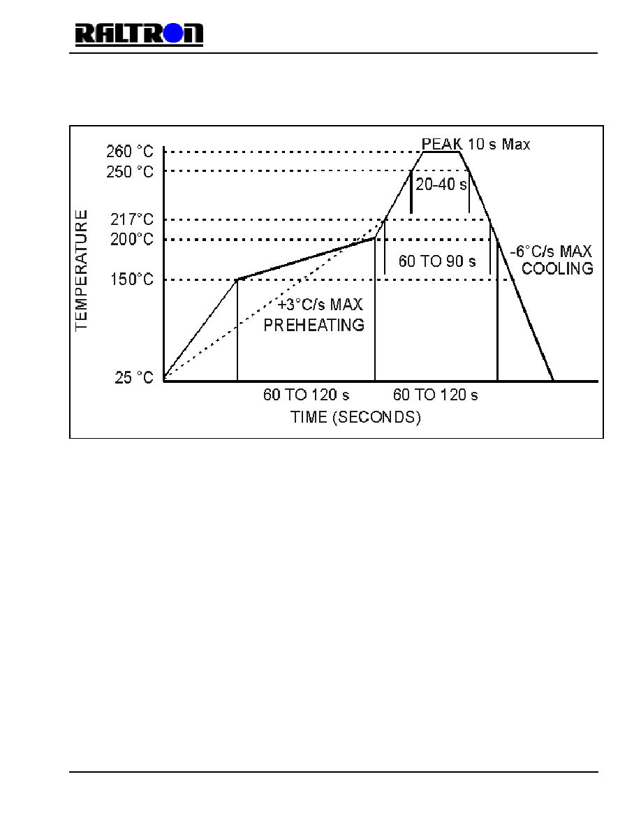
*1 Test Conditions Unless Stated Otherwise: Nominal Vcc, Nominal Load, +25
±
3
∞
C
*2 Frequency Dependent
*3 Not All Stabilities Available With All Temperature Ranges--Please Consult Factory For Availability
*
4 Measured with Wavecrest SIA-3000A 1,000,000 Hits no filtering
*5 Calculated from Agilent 5500 phase noise measurements
*6 Measured with Agilent 5500
$
$
$
$
PART NUMBERING SYSTEM:
SERIES
SYMMETRY
TEMPERATURE
RANGE (∞C)
FREQUENCY
STABILITY
(Overall)
FREQUENCY
(MHz)
CS9L: UHF +3.3Vdc Clock with PECL Comp. Output
CSPL: UHF +2.5Vdc Clock with PECL Comp. Output
A: 40/60 to 60/40%
T: 45/55 to 55/45%
R: 0...+50
S: 0...+70
U: -20...+70
V: -40...+85**
K:
±
20 ppm**
I:
±
25 ppm**
H:
±
50 ppm
J:
±
100 ppm
150.000...700.000
EXAMPLE: CS9LASH-155.520
Clock Oscillator, 7x5mm Package, +3.3 VDC Supply Voltage, PECL Output, Standard Symmetry, 0...+70
∞
C Operating
Temperature Range,
±
50 ppm Total Frequency Stability, 155.520 MHz
**Above 300MHz extended temp range and ±25ppm stability may not be available, jitter may vary upon spec requirements.
Please consult the factory for any custom requirements.
$
$
$
$
MECHANICAL PARAMETERS:
OUTLINE TOLERANCE:
±0.006" / 0.15mm
(Unless otherwise specified)
PIN FUNCTIONS:
[1] ENABLE/ DISABLE
[2] NO CONNECT
[3] CASE GROUND
[4] OUTPUT
[5] COMP. OUTPUT
[6] SUPPLY VOLTAGE
MARKING:
CS9LASH
155.52
RAL D/C
*0.01
µ
µ
µ
µ
F external by-pass
filter is recommended as seen on solder
pattern.