
SYNCHRONOUS EQUIPMENT
LOW INPUT/ HIGH DUAL OUTPUT FREQUENCY CLOCK/SYNCHRONIZER
SY02-HP2O
RALTRON ELECTRONICS CORP.
ß
10651 N.W.19
th
St
ß
Florida 33172
ß
U.S.A.
Tel: 305 593-6033
ß
Fax: 305-594-3973
ß
e-mail: sales@raltron.com
ß
Internet: http://www.raltron.com
1
August 13, 2004
∑
INTRODUCTION
The SY02-HP2O is a high frequency crystal-based PLL synchronizer designed as a module level subsystem for easy
incorporation into telecommunication equipment.
∑
FEATURES
-
Low jitter output from intrinsically low jitter VCXO or VCSO;
-
One pre-selected input reference of
8kHz to 77.76MHz
(CMOS levels);
-
Two pairs of high frequency differential LVPECL outputs up to
800MHz
. (must be at the same frequency)
-
Alarms and status;
-
Provides free running clock output;
-
The unit changes timing modes in response to external events;
-
J-TAG service port for re-programming and servicing;
-
3.3V DC power supply
-
Small dimensions: 0.75" x 1.20" SMT pkg.
∑
APPLICATIONS
-
ATM
-
SDH
-
PDH
-
SONET
-
Other telecommunication equipment.
SYNCHRONOUS EQUIPMENT
LOW INPUT/ HIGH DUAL OUTPUT FREQUENCY CLOCK/SYNCHRONIZER
SY02-HP2O
RALTRON ELECTRONICS CORP.
ß
10651 N.W.19
th
St
ß
Florida 33172
ß
U.S.A.
Tel: 305 593-6033
ß
Fax: 305-594-3973
ß
e-mail: sales@raltron.com
ß
Internet: http://www.raltron.com
2
∑
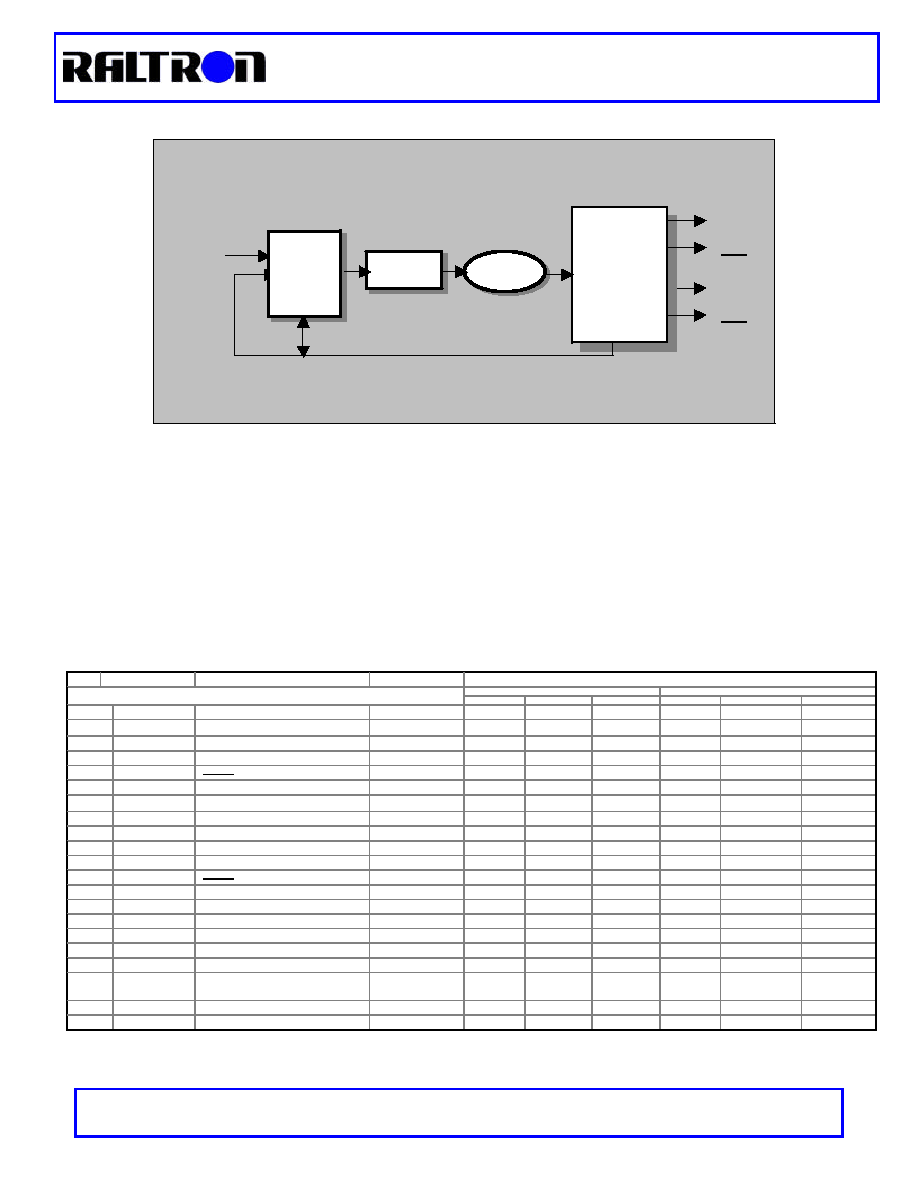
DESCRIPTION
The SY02-HP2O is a High Frequency Phase Lock Loop has been designed as a module level subsystem for easy
incorporation into telecommunication equipment. The module generates the high frequency (up to 800.00MHz) output
from a low jitter VCXO or VCSO (SAW based oscillators). The SY02-HP2O can be locked to one reference of a pre-
selected input frequency between 8 kHz to 77.76MHz. The module has fast locking time and tolerates reference
inputs with different duty cycles. The loop bandwidth is optimized according to used VCXO and wanted output
performance. The SMD package dimensions are 0.75x1.20 inch and power supply is 3.3V. Parts are assembled using
high temperature solder to withstand surface mount reflow process.
∑
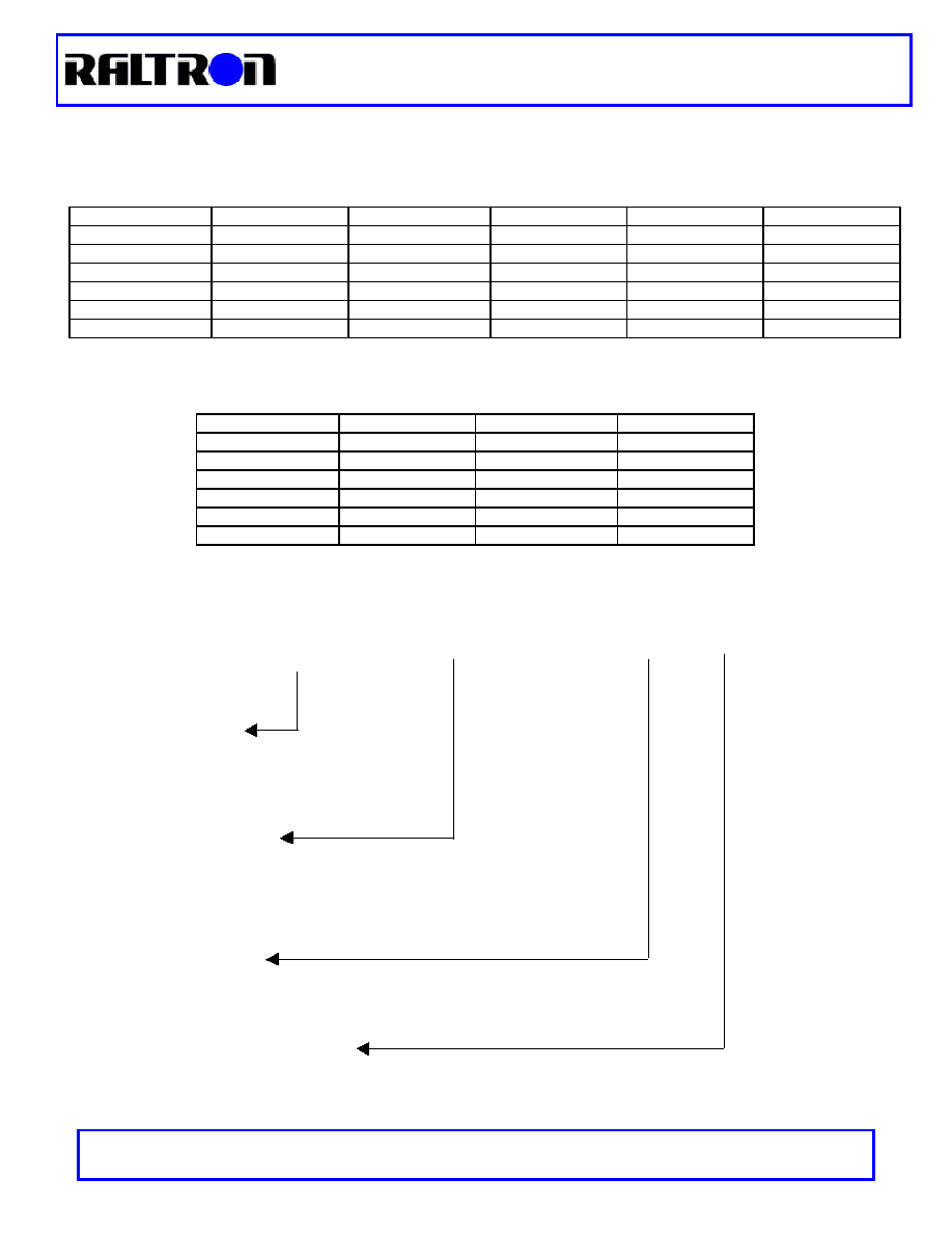
PIN DESCRIPTION
Name
Description
Signal Technology
VL
VH/ DC Voltage
Min
Typ
Max
Min
Typ
Max
1
1
NC
-----
-----
-----
----
------
------
------
2
2
REF IN
HCMOS
(3.3 Tolerable)
0
-----
0.5
(0.3)
4.5
(2.97)
----
----
3
**3
TDO
-----
-----
-----
----
------
------
------
4
4
GND
-----
-----
-----
----
------
------
------
5
5
OUT 1
LV/PECL
Vcc-1.680
Vcc-1.620
Vcc-1.560
Vcc-1.085
Vcc-1.025
Vcc-0.885
6
6
OUT 1
LV/PECL
Vcc-1.680
Vcc-1.620
Vcc-1.560
Vcc-1.085
Vcc-1.025
Vcc-0.885
7
7
Vcc
DC ≠ 5V
(3.3V)
4.5
(2.97)
5.0
(3.3)
5.25
(3.465)
8
8
GND
-----
-----
-----
----
------
------
------
9
9
NC
-----
-----
-----
----
------
------
------
10
10
NC
-----
-----
-----
----
------
------
------
11
11
OUT 2
LV/PECL
Vcc-1.680
Vcc-1.620
Vcc-1.560
Vcc-1.085
Vcc-1.025
Vcc-0.885
12
12
OUT 2
LV/PECL
Vcc-1.680
Vcc-1.620
Vcc-1.560
Vcc-1.085
Vcc-1.025
Vcc-0.885
13
13
GND
-----
-----
-----
----
------
------
------
14
14
GND
-----
-----
-----
----
------
------
------
15
15
Vcc
3.3V
2.97
3.3
3.465
16
**16
TDI
-----
-----
-----
----
------
------
------
17
**17
TCK
-----
-----
-----
----
------
------
------
18
**18
TMS
-----
-----
-----
----
------
------
------
**18
TMS
J-TAG port for factory usage ≠
TMS
-----
-----
-----
----
------
------
------
19
GND
Ground
-----
-----
-----
----
------
------
------
20
NC
Not Connected
-----
-----
-----
----
------
------
------
**
Do not Connect Pin
LOOP
FILTER
VCXO
MUX,
FPD,
Counter
s &
Logic
OUT 1
J-TAG PORT
REF IN
LVPECL
DIVIDER
OUT 2
OUT 1
OUT 2
SYNCHRONOUS EQUIPMENT
LOW INPUT/ HIGH DUAL OUTPUT FREQUENCY CLOCK/SYNCHRONIZER
SY02-HP2O
RALTRON ELECTRONICS CORP.
ß
10651 N.W.19
th
St
ß
Florida 33172
ß
U.S.A.
Tel: 305 593-6033
ß
Fax: 305-594-3973
ß
e-mail: sales@raltron.com
ß
Internet: http://www.raltron.com
3
∑
ORDERING INFORMATION
o
Input Frequencies available;
Frequency
Suffix
Frequency
Suffix
Frequency
Suffix
8KHz
F8
19.44MHz
O1
77.76MHz
O3
1.544MHz
T1
24.704MHz
T3
2.048MHz
E1
32.768MHz
E4
8.192MHz
E3
38.88MHz
O2
12.352MHz
T4
51.84MHz
D2
16.384MHz
E4
62.50MHz
G5
o
Output Frequencies available (in MHz);
Frequency
Suffix
Frequency
Suffix
51.84
D2
156.25
G6
62.50
G5
166.1328
B9
77.76
O3
622.08
O6
125
G2
666.5143
C10
133
G4
155.52
O4
ÿ
P/N System
SY02-HP2O≠ IP < Input Frequency> - OU1&2<Output Frequency>- S-T<Temp. Range>
ÿ
See above Chart
(If not listed Place
NL
and state the Freq.)
ÿ
See above Chart
(If Output Freq. Not applied place
NA
and state the Freq.)
ÿ
Supply Voltage;
2
- 5V
4
≠ 3.3V
ÿ
Operating Temperature Range;
C
-
0∞C to 70∞C
I
-
-40∞C to +85∞C
-
For other frequencies contact the factory!
SYNCHRONOUS EQUIPMENT
LOW INPUT/ HIGH DUAL OUTPUT FREQUENCY CLOCK/SYNCHRONIZER
SY02-HP2O
RALTRON ELECTRONICS CORP.
ß
10651 N.W.19
th
St
ß
Florida 33172
ß
U.S.A.
Tel: 305 593-6033
ß
Fax: 305-594-3973
ß
e-mail: sales@raltron.com
ß
Internet: http://www.raltron.com
4
∑
SPECIFICATION
General
Specifications
Mechanical 0.75" x 1.20"
SMT Module FR4 20 pins dual-in-line, withstand SMD
reflow process.
Power 3.3VDC+/-5%, <200mA
Regulated
Environment Operating Temperature
0∞C to 70∞C
Humidity
5% to 95% non-condensing
Internal Oscillators VCXO or VCSO
Depend of the frequency
Input Signals
Number of Reference Inputs 1
Input reference frequency 8kHz to 77.76MHz
Signal Level HCMOS/TTL Compatible
Output Signals
Number of Outputs 2
Output 1 See above Table
Other frequency contact Raltron
Output 1 Signal Level LVPECL
50%+/-10% (std Duty Cycle); 50%+/-5% (upon
request)
Rise/Fall Time 350pS max (@ 155.52MHz)
VOH - 2.272Vdc min; VOL ≠ 1.68Vdc max.
Tracking/Capture Range
±
25ppm min
Signal Quality
Performance
Jitter generation <1pS RMS, 10ps pk-pk
Jitter based on SONET OC-48 B.W - 12KHz to 20MHz
Jitter tolerance 2
µ
s, 10 Hz (0.05UI @ 8kHz)
Input Jitter tolerance 6.25uS max.
∑
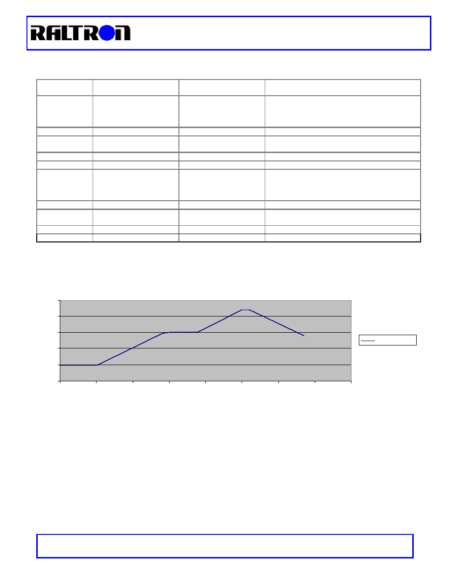
REFLOW PROFILE
0
50
100
150
200
250
0
1
2
3
4
5
6
7
8
XY (Scatter) 1
SYNCHRONOUS EQUIPMENT
LOW INPUT/ HIGH DUAL OUTPUT FREQUENCY CLOCK/SYNCHRONIZER
SY02-HP2O
RALTRON ELECTRONICS CORP.
ß
10651 N.W.19
th
St
ß
Florida 33172
ß
U.S.A.
Tel: 305 593-6033
ß
Fax: 305-594-3973
ß
e-mail: sales@raltron.com
ß
Internet: http://www.raltron.com
5
∑
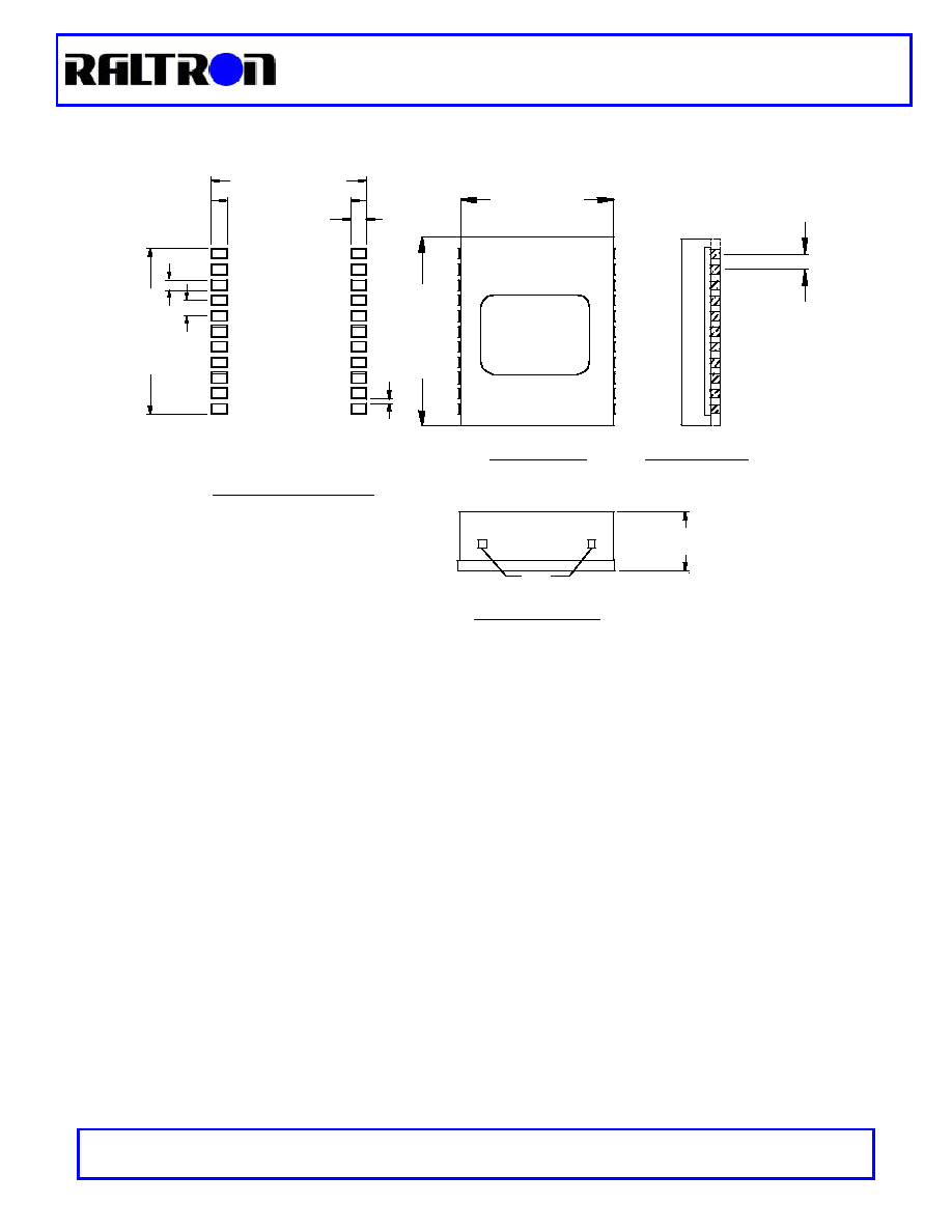
OUTLINE DRAWING
LABEL
MARKING
FRONT VIEW
10
11
TOP VIEW
SIDE VIEW
TABS
1
20
.100
.750 (19.05 mm)
1.20 (30.48 mm)
PCB FOOTPRINT
.800 TYP. (20.32 mm)
.100 (.2.54 mm)
.950 (24.13 mm)
.050 TYP (1.27 mm)
.080 TYP (2.03 mm)
.640 TYP.(16.26 mm)
.050 TYP (1.27 mm)
.376