
This product conforms specifications per the terms of the Ramtron
Ramtron International Corporation
standard warranty. Production processing does not necessarily
1850 Ramtron Drive, Colorado Springs, CO 80921
include testing of all parameters.
(800) 545-FRAM, (719) 481-7000, Fax (719) 481-7058
www.ramtron.com
Rev 1.2
Jan. 2002
Page 1of 13
FM24C256
256Kb FRAM Serial Memory
Features
256Kbit Ferroelectric Nonvolatile RAM
∑
Organized as 32,768 x 8 bits
∑
High Endurance 10 Billion (10
10
) Read/Writes
∑
10 year Data Retention
∑
NoDelayTM Writes
∑
Advanced High-Reliability Ferroelectric Process
Fast Two-wire Serial Interface
∑
Up to 1 MHz Maximum Bus Frequency
∑
Supports Legacy Timing for 100 kHz & 400 kHz
Low Power Operation
∑
5V Operation
∑
200
µ
A Active Current (100 kHz)
∑
100
µ
A Standby Current
Industry Standard Configuration
∑
Industrial Temperature -40
∞
C to +85
∞
C
∑
8-pin EIAJ SOP
Description
The FM24C256 is a 256-kilobit nonvolatile memory
employing an advanced ferroelectric process. A
ferroelectric random access memory or FRAM is
nonvolatile and performs reads and writes like a
RAM. It provides reliable data retention for 10 years
while eliminating the complexities, overhead, and
system level reliability problems caused by
EEPROM and other nonvolatile memories.
The FM24C256 performs write operations at bus
speed. No write delays are incurred. The next bus
cycle may commence immediately without the need
for data polling. In addition, the product offers write
endurance orders of magnitude higher than
EEPROM. Also, FRAM exhibits much lower power
during writes than EEPROM since write operations
do not require an internally elevated power supply
voltage for write circuits.
These capabilities make the FM24C256 ideal for
nonvolatile memory applications requiring frequent
or rapid writes. Examples range from data collection
where the number of write cycles may be critical, to
demanding industrial controls where the long write
time of EEPROM can cause data loss. The
combination of features allows more frequent data
writing with less overhead for the system.
The FM24C256 is available in a 8-pin EIAJ SOP
package using an industry standard two-wire
protocol. Specifications are guaranteed over an
industrial temperature range of -40∞C to +85∞C.
Pin Configuration
A0
A1
A2
VSS
VDD
WP
SCL
SDA
1
2
3
4
8
7
6
5
Pin Names
Function
A0-A2
Device Select Address
SDA Serial
Data/Address
SCL Serial
Clock
WP Write
Protect
VSS Ground
VDD
Supply Voltage 5V
Ordering Information
FM24C256-SE
8-pin EIAJ SOP
FM24C256
Rev 1.2
Jan. 2002
Page 2 of 13
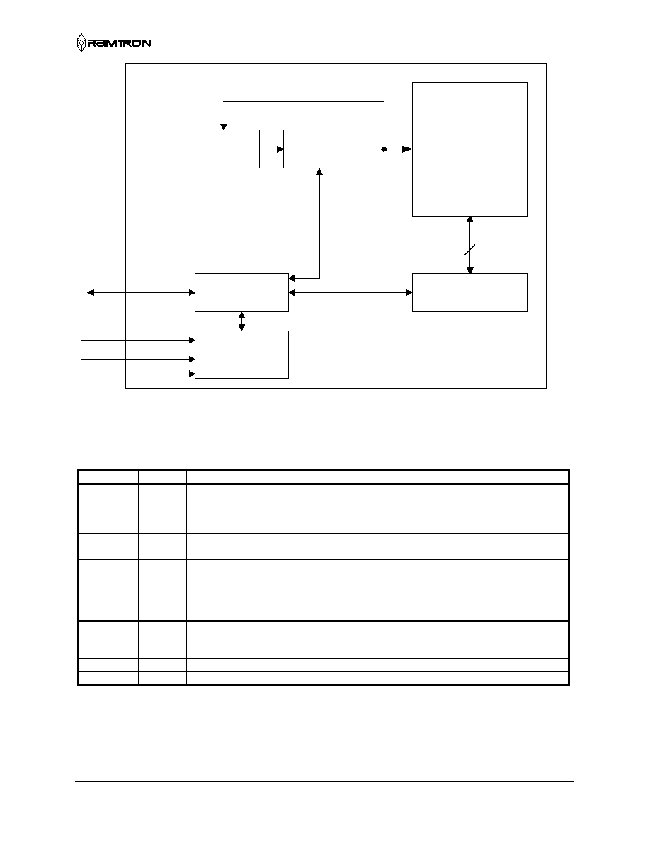
Address
Latch
`
4,096 x 64
FRAM Array
Data Latch
8
SDA
Counter
Serial to Parallel
Converter
Control Logic
SCL
WP
A0-A2
Figure 1. Block Diagram
Pin Description
Pin Name
Type
Pin Description
A0-A2
Input
Address 2-0: These pins are used to select one of up to 8 devices of the same type on
the same two-wire bus. To select the device, the address value on the three pins must
match the corresponding bits contained in the device address. The address pins are
pulled down internally.
WP
Input
Write Protect: When WP is high, the entire array will be write-protected. When WP is
low, all addresses may be written. This pin is internally pulled down.
SDA
I/O
Serial Data/Address: This is a bi-directional input used to shift serial data and
addresses for the two-wire interface. It employs an open-drain output and is intended
to be wire-OR'd with other devices on the two-wire bus. The input buffer incorporates
a Schmitt trigger for improved noise immunity and the output driver has slope control
for falling edges. An external pull-up resistor is required.
SCL
Input
Serial Clock: The serial clock input for the two-wire interface. Data is clocked out of
the device on the SCL falling edge, and clocked in on the SCL rising edge. The SCL
input also incorporates a Schmitt trigger input for improved noise immunity.
VDD
Supply
Supply Voltage: 5V
VSS Supply
Ground

FM24C256
Rev 1.2
Jan. 2002
Page 3 of 13
Overview
The FM24C256 is a serial FRAM memory. The
memory array is logically organized as 32,768 x 8 bit
memory array and is accessed using an industry
standard two-wire interface. Functional operation of
the FRAM is similar to serial EEPROMs. The major
difference between the FM24C256 and a serial
EEPROM relates to its superior write performance.
Memory Architecture
When accessing the FM24C256, the user addresses
32,768 locations each with 8 data bits. These data bits
are shifted serially. The 32,768 addresses are
accessed using the two-wire protocol, which includes
a slave address (to distinguish from other non-
memory devices), and an extended 16-bit address.
Only the lower 15 bits are used by the decoder for
accessing the memory. The upper address bit should
be set to 0 for compatibility with higher density
devices in the future.
The memory is read or written at the speed of the
two-wire bus. Unlike an EEPROM, it is not
necessary to poll the device for a ready condition
since writes occur at bus speed. By the time a new
bus transaction can be shifted into the part, a write
operation is complete. This is explained in more
detail in the interface section below.
Users can expect several obvious system benefits
from the FM24C256 due to its fast write cycle and
high endurance as compared with EEPROM.
However there are less obvious benefits as well. For
example in a high noise environment, the fast-write
operation is less susceptible to corruption than an
EEPROM since the write cycle is completed quickly.
By contrast, an EEPROM requiring milliseconds to
write is vulnerable to noise during much of the cycle.
Note that the FM24C256 contains no power
management circuits other than a simple internal
power-on reset. It is the user's responsibility to
ensure that V
DD
is maintained within data sheet
tolerances to prevent incorrect operation.
Two-wire Interface
The FM24C256 employs a bi-directional two-wire
bus protocol using few pins and little board space.
Figure 2 illustrates a typical system configuration
using the FM24C256 in a microcontroller-based
system. The industry standard two-wire bus is
familiar to many users but is described in this section.
By convention, any device that is sending data onto
the bus is the transmitter while the target device for
this data is the receiver. The device that is controlling
the bus is the master. The master is responsible for
generating the clock signal for all operations. Any
device on the bus that is being controlled is a slave.
The FM24C256 is always a slave device.
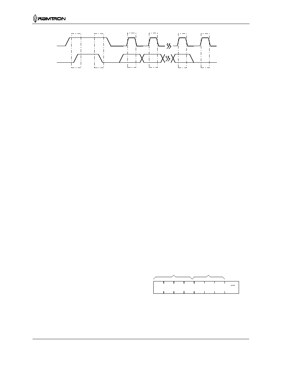
The bus protocol is controlled by transition states in
the SDA and SCL signals. There are four conditions
including Start, Stop, Data bit, and Acknowledge.
Figure 3 illustrates the signal conditions that specify
the four states. Detailed timing diagrams are shown
in the electrical specifications.
Microcontroller
SDA
SCL
FM24C256
A0 A1 A2
SDA
SCL
FM24C64
A0 A1 A2
VDD
Rmin = 1.8 K
Rmax = tR/Cbus
Figure 2. Typical System Configuration
FM24C256
Rev 1.2
Jan. 2002
Page 4 of 13
Stop
(Master)
Start
(Master)
7
Data bits
(Transmitter)
6
0
Data bit
(Transmitter)
Acknowledge
(Receiver)
Figure 3. Data Transfer Protocol
Stop Condition
A Stop condition is indicated when the bus master
drives SDA from low to high while the SCL signal is
high. All operations using the FM24C256 must end
with a Stop condition. If an operation is pending
when a Stop is asserted, the operation will be aborted.
The master must have control of SDA (not a memory
read) in order to assert a Stop condition.
Start Condition
A Start condition is indicated when the bus master
drives SDA from high to low while the SCL signal is
high. All read and write transactions begin with a
Start condition. An operation in progress can be
aborted by asserting a Start condition at any time.
Aborting an operation using the Start condition will
ready the FM24C256 for a new operation.
If during operation the power supply drops below the
specified VDD minimum, the system should issue a
Start condition prior to performing another operation.
Data/Address Transfer
All data transfers (including addresses) take place
while the SCL signal is high. Except under the two
conditions described above, the SDA signal should
not change while SCL is high.
Acknowledge
The Acknowledge takes place after the 8
th
data bit
has been transferred in any transaction. During this
state the transmitter should release the SDA bus to
allow the receiver to drive it. The receiver drives the
SDA signal low to acknowledge receipt of the byte.
If the receiver does not drive SDA low, the condition
is a No-Acknowledge and the operation is aborted.
The receiver would fail to acknowledge for two
distinct reasons. First is that a byte transfer fails. In
this case, the No-Acknowledge ends the current
operation so that the part can be addressed again.
This allows the last byte to be recovered in the event
of a communication error.
Second and most common, the receiver does not
acknowledge to deliberately end an operation. For
example, during a read operation, the FM24C256
will continue to place data onto the bus as long as
the receiver sends Acknowledges (and clocks).
When a read operation is complete and no more data
is needed, the receiver must not acknowledge the
last byte. If the receiver acknowledges the last byte,
this will cause the FM24C256 to attempt to drive
the bus on the next clock while the master is sending
a new command such as Stop.
Slave Address
The first byte that the FM24C256 expects after a
Start condition is the slave address. As shown in
Figure 4, the slave address contains the Slave ID
(device type), the device select address bits, and a
bit that specifies if the transaction is a read or a
write. Bits 7-4 define the device type and must be
set to 1010b for the FM24C256. These bits allow
other types of function types to reside on the 2-wire
bus within an identical address range. Bits 3-1 are
the device select bits which are equivalent to chip
select bits. They must match the corresponding
value on the external address pins to select the
device. Up to eight FM24C256 devices can reside
on the same two-wire bus by assigning a different
address to each. Bit 0 is the read/write bit. A 1
indicates a read operation, and a 0 indicates a write.
1
0
1
0
A2 A1 A0 R/W
Slave
ID
Device
Select
7
6
5
4
3
2
1
0
Figure 4. Slave Address

FM24C256
Rev 1.2
Jan. 2002
Page 5 of 13
Addressing Overview
After the FM24C256 (as receiver) acknowledges the
device address, the master can place the memory
address on the bus for a write operation. The address
requires two bytes. The first is the MSB (upper byte).
Since the device uses only 15 address bits, the value
of the upper bits is a "don't care". Following the
MSB is the LSB (lower byte) with the remaining
eight address bits. The address value is latched
internally. Each access causes the latched address
value to be incremented automatically. The current
address is the value that is held in the latch, either a
newly written value or the address following the last
access. The current address will be held as long as
power remains or until a new value is written. Reads
always use the current address. A random read
address can be loaded by beginning a write operation
as explained below.
After transmission of each data byte, just prior to the
acknowledge, the FM24C256 increments the internal
address latch. This allows the next sequential byte to
be accessed with no additional addressing externally.
After the last address (7FFFh) is reached, the address
latch will roll over to 0000h. There is no limit to the
number of bytes that can be accessed with a single
read or write operation.
Data Transfer
After the address information has been transmitted,
data transfer between the bus master and the
FM24C256 can begin. For a read operation the
FM24C256 will place 8 data bits on the bus then wait
for an Acknowledge from the master. If the
Acknowledge occurs, the FM24C256 will transfer the
next sequential byte. If the Acknowledge is not sent,
the FM24C256 will end the read operation. For a
write operation, the FM24C256 will accept 8 data
bits from the master then send an acknowledge. All
data transfer occurs MSB (most significant bit) first.
Memory Operation
The FM24C256 is designed to operate in a manner
very similar to other 2-wire interface memory
products. The major differences result from the
higher performance write capability of FRAM
technology. These improvements result in some
differences between the FM24C256 and a similar
configuration EEPROM during writes. The complete
operation for both writes and reads is explained
below.
Write Operation
All writes begin with a device address, then a
memory address. The bus master indicates a write
operation by setting the LSB of the device address
to a 0. After addressing, the bus master sends each
byte of data to the memory and the memory
generates an acknowledge condition. Any number of
sequential bytes may be written. If the end of the
address range is reached internally, the address
counter will wrap from 7FFFh to 0000h.
Unlike other nonvolatile memory technologies,
there is essentially no write delay with FRAM.
Since the read and write access times of the
underlying memory are the same, the user
experiences no delay on the bus. The entire memory
cycle occurs in less time than a single bus clock.
Therefore, any operation including a read or write
can occur immediately following a write.
Acknowledge polling, a technique used with
EEPROMs to determine if a write has completed is
unnecessary and will always return a ready
condition.
Internally, an actual memory write occurs after the
8
th
data bit is transferred. It will be complete before
the Acknowledge is sent. Therefore, if the user
desires to abort a write without altering the memory
contents, this should be done using a Start or Stop
condition prior to the 8
th
data bit. The FM24C256
uses no page buffering.
The memory array can be write protected using the
WP pin. Pulling the WP pin high will write-protect
all addresses. The FM24C256 will not acknowledge
data bytes that are written when WP is active. In
addition, the address counter will not increment if
writes are attempted to these addresses. Setting WP
low will deactivate this feature. WP is internally
pulled down. The state of WP should remain stable
from the Start command until the address is
complete.
Figure 5 and 6 below illustrate both a single-byte
and multiple-write.