
Raytheon RF Components
362 Lowell Street
Andover, MA, USA 01810
Revised March 28, 2003
Page 1
www.raytheonrf.com
Specifications are based on most current or latest revision.
Raytheon
RF Components
RMPA2550-252
2.4-2.5 GHz and 5.15-5.35 GHz Dual Band InGaP
HBT Linear Power Amplifier
ADVANCED INFORMATION
Description
Features
Absolute
Ratings
1
Electrical
Characteristics
2.4 ≠ 2.5 GHz
2
The RMPA2550-252 is a dual frequency band power amplifier designed for high performance WLAN
applications in the 2.4 - 2.5 GHz and the 5.15 - 5.35 GHz frequency bands. The single low profile 20 pin
3 x 4 mm package with internal matching on both input and output to 50 Ohms minimizes next level
PCB space and allows for simplified integration. The two on-chip detectors provide power sensing
capability while the logic control provides power saving shutdown options.
The PA's low power
consumption and excellent linearity are achieved using Raytheon RF Components' InGaP
Heterojunction Bipolar Transistor (HBT) technology.
Parameter
Symbol
Value
Units
Positive Supply Voltage
VC
6
V
Supply Current
IC 2.4
820
mA
IC 5.0
700
mA
Voltage Mirror
VM
5
V
Logic Voltage
V
L
5
V
RF Input Power
P
in
10
dBm
Case Operating Temperature
T
Case
-40 to +85
∞
C
Storage Temperature
T
stg
-55 to +150
∞
C
!
Dual band operation in a single package design
!
> 26 dB small signal gain both frequency bands
!
> 26 dBm output power @ 1 dB compression both frequency bands
!
4% EVM at 19 dBm Pout, 2.45 GHz; 2% EVM at 18 dBm Pout, 5.25 GHz
!
3.3 V single positive supply operation
!
Adjustable bias current operation
!
Two power saving shutdown options (bias and logic control)
!
Separate integrated power detectors with 20 dB dynamic range
!
Low profile 20 pin, 3 x 4 x 1 mm standard QFN leadless package
!
Internally matched to 50 ohms
!
Optimized for use in 802.11a/b/g applications
Parameter
Minimum
Typical
Maximum
Unit
Frequency
2.4
2.5
GHz
Supply Voltage
3.0
3.3
3.6
V
Gain
24.5
26
30
dB
P1dB Compression
25
26.5
dBm
Quiescent Current
70
110
135
mA
Standby Current
3
0.7
mA
Shutdown Current
4
<1
µ
A
Current @ P1dB Comp
365
425
mA
EVM
5
Po=16 dBm, Ic=135 mA
2
3
%
Po=19 dBm, Ic=155 mA
4
7
%
Input Return Loss
15
dB
Output Return Loss
12
dB
Detector Output
0 ≠ 3
V
2
nd
Harmonic Output (P1dB)
-45
dBc
Logic Shutdown Control
(VL 2.4):
Device Off, Logic High
2.4
V
Device On, Logic Low
0.5
V
Logic Current
150
µ
A
Turn-on Time
<1
µ
S
Turn-off Time
<1
µ
S
Note:
1. No permanent damage with only one parameter set at extreme limit. Other parameters set to typical values.
2. VC1 2.4,VC2 2.4, VM 2.4= 3.3 Volts, Tc=25
∞
C
3. Standby current when shutdown from logic input.
4. Shutdown current when supply voltage is disabled.
5. Percentage increase above system noise floor, 802.11g, OFDM, 54 Mbps. EVM not measured 100% in production.
Raytheon RF Components
362 Lowell Street
Andover, MA, USA 01810
Revised March 28, 2003
Page 2
www.raytheonrf.com
Specifications are based on most current or latest revision.
Raytheon
RF Components
RMPA2550-252
2.4-2.5 GHz and 5.15-5.35 GHz Dual Band InGaP
HBT Linear Power Amplifier
ADVANCED INFORMATION
Parameter
Minimum
Typical
Maximum
Unit
Frequency
5.15
5.35
GHz
Supply Voltage
3.0
3.3
3.6
V
Gain
27
dB
P1dB Compression
26
dBm
Quiescent Current
2
140-200
mA
Standby Current
3
1.9
mA
Shutdown Current
4
<1
µ
A
Current @ P1dB Comp
450
mA
EVM
5
Po=18dBm, Ic=240mA
2
%
Input Return Loss
12
dB
Output Return Loss
10
dB
Detector Output
0 ≠ 1.3
V
Harmonic Output
6
-30
dBc
Logic Shutdown
Control (VL 5.0):
Device On, Logic High
2.4
V
Device Off, Logic Low
0.5
V
Logic Current
150
µ
A
Turn-on Time
<1
µ
S
Turn-off Time
<1
µ
S
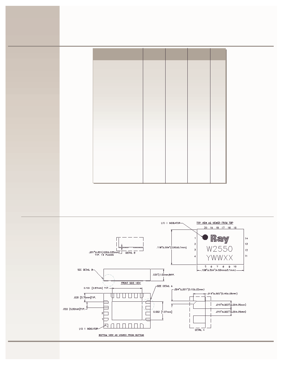
Package Outline
Dimensions in inches [mm]
Electrical
Characteristics
Continued
5.15 ≠ 5.35 GHz
1
Note:.
1. VC1 5.0, VC2 5.0, VC3 5.0, VM13 5.0, VM2 5.0 = 3.3 Volts, Tc=25
∞
C
2. See data on pages 10, 11.
3. Standby current when shutdown from logic input.
4. Shutdown current when supply voltage is disabled.
5. Percentage increase above system noise floor, 802.11a, OFDM, 54 Mbps. EVM not measured 100% in production.
6. At Pout=20 dBm

Raytheon RF Components
362 Lowell Street
Andover, MA, USA 01810
Revised March 28, 2003
Page 3
www.raytheonrf.com
Specifications are based on most current or latest revision.
Raytheon
RF Components
RMPA2550-252
2.4-2.5 GHz and 5.15-5.35 GHz Dual Band InGaP
HBT Linear Power Amplifier
ADVANCED INFORMATION
Functional
Block Diagram
Pin
1
2
3
4
5
6
7
8
9
10
11
12
13
14
15
16
17
18
19
20
Description
VM 2.4
DT2 2.4
DT1 2.4 (Vdet)
VC2 2.4
N/C
RF OUT 2.4
N/C
N/C
RF OUT 5.0
DT1 5.0 (Vdet)
VC3 5.0
VC2 5.0
VM2 5.0
VL 5.0
VM13 5.0
VC1 5.0
RF IN 5.0
VC1 2.4
RF IN 2.4
VL 2.4
Backside Ground
Bias
5.0 GHz
PA
2.4 GHz
PA
Bias
Evaluation
Board Layout
Actual Board Size
= 2.0" X 1.5"
Output
Match
Detector
Output
Match
Input
Match
Bias
Detector
Input
Match
J2
J4
J3
J1

Raytheon RF Components
362 Lowell Street
Andover, MA, USA 01810
Revised March 28, 2003
Page 4
www.raytheonrf.com
Specifications are based on most current or latest revision.
Raytheon
RF Components
RMPA2550-252
2.4-2.5 GHz and 5.15-5.35 GHz Dual Band InGaP
HBT Linear Power Amplifier
ADVANCED INFORMATION
Evaluation
Board Schematic
Evaluation
Board Bill
of Materials
Backside Ground

Raytheon RF Components
362 Lowell Street
Andover, MA, USA 01810
Revised March 28, 2003
Page 5
www.raytheonrf.com
Specifications are based on most current or latest revision.
Raytheon
RF Components
RMPA2550-252
2.4-2.5 GHz and 5.15-5.35 GHz Dual Band InGaP
HBT Linear Power Amplifier
ADVANCED INFORMATION
Evaluation Board
Turn-On
Sequence
1
Recommended turn-on sequence 2.4 ≠2.5 GHz Band:
1) Connect RF ports J3, J4 to RF test equipment.
2) Connect common ground terminal to the Ground (GND) pin on the board.
3) Connect logic control pin VL 2.4 to positive supply.
4) Connect terminals VC1 2.4, VC2 2.4 together and connect to positive supply
5) Connect terminal VM 2.4 to positive supply.
6) Connect voltmeter to Detector Output, pin DT1 2.4.
7) Apply low voltage of 0.0 to +0.5 V to logic control pin VL 2.4. (On)
8) Apply positive voltage of 3.3 V to pin VC1 2.4 and VC2 2.4 (first & second stage collector).
9) Apply positive voltage of 3.3 V to pin VM 2.4 (bias networks)
2
.
10) At this point, you should expect to observe the following positive currents flowing into the pins:
Pin
Current
VL 2.4
<1 nA
VC1 2.4
40.0 - 55.0 mA
VC2 2.4
45.0 - 55.0 mA
VM 2.4
12.0 - 15.0 mA
11) Apply input RF power to SMA connector pin RF IN 2.4. Currents on collector pins will vary depending on the input
drive level.
12) Vary positive voltage VL 2.4 from +0.5 V to +2.4 V to shut down the amplifier or alter the power level. Shut down
current flow into the pins:
Pin
Current
VL 2.4
<0.25 mA
VC1 2.4
<1 nA
VC2 2.4
<1 nA
VM 2.4
< 0.7 mA
Recommended turn-off sequence:
Use reverse order described in the turn-on sequence above.
Note:
1.
Turn on sequence is not critical and it is not necessary to sequence power supplies in actual system level design.
2.
VM may be adjusted from +2.9 to +3.3V to adjust bias current operation.