128
www.recom-international.com
24-August-2005
2, 3, 4, 5 AMP
SIP12
Vertical
&
&
Horizontal
INNOLINE
DC/DC-Converter
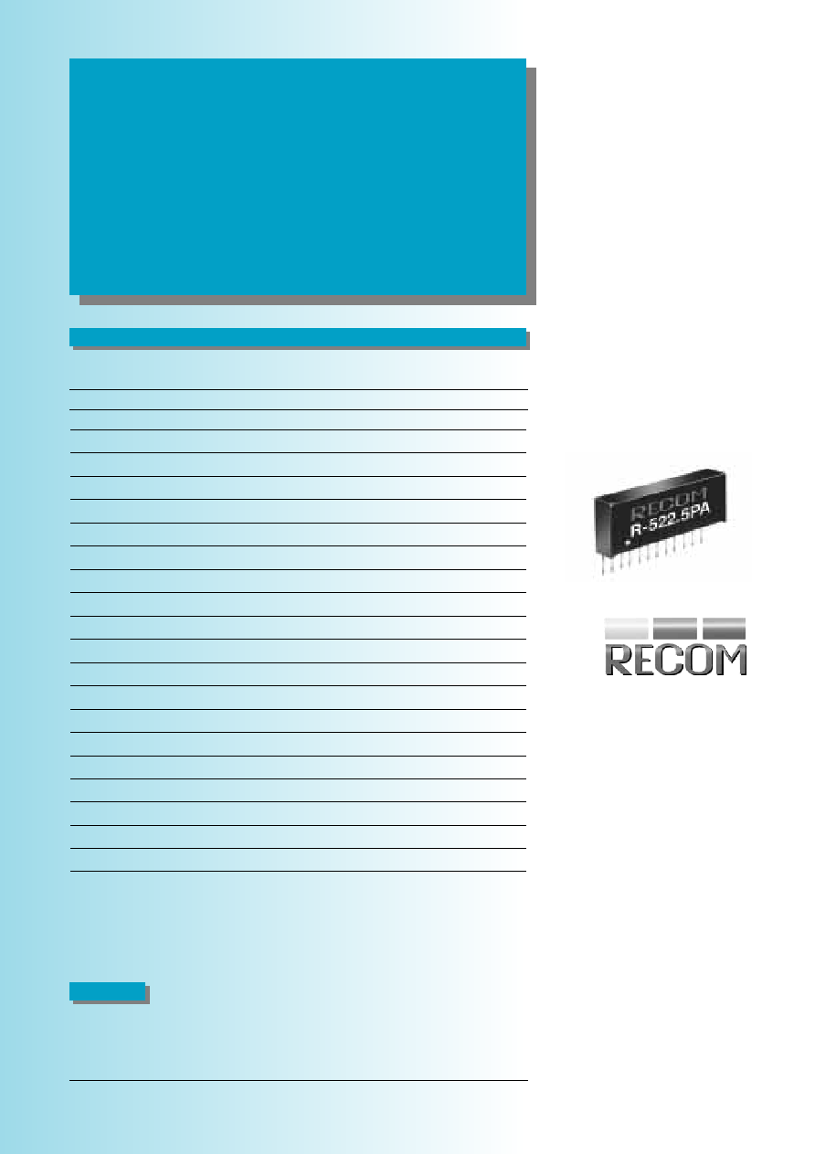
R-5xxxPA
_DA Series
Auto-sense
Non-Isolation
Synchronous rectification design
Adjustable Output voltage
2, 3, 4 & 5AMP Adjustable Positive
Step Down Integrated Switching Regulator
Over load protection (125% full load typical)
Remote ON/OFF Control(Ground Off)
Wide Input Range
Continuous short circuit protection
(Very low short input current: Iin<50mA)
Input voltage range 4.5V~18V
Efficiency to 96%
Features
Selection Guide
Part
Inpu
Nominal
Vout
Output Efficiency
(%)
Number
Range
Output Voltage
Adjust Range
Current
min
max
SIP12
(V)
(V)
(V)
(A)
Vin
12V
Vin
R-521.2xA
4.5 � 18
1.2
1.0 � 3.0
2
83
79
75
R-521.8xA
4.5 � 18
1.8
1.1 � 4.5
2
88
85
82
R-522.5xA
4.5 � 18
2.5
1.6 � 5.5
2
91
88
86
R-523.3xA
4.5 � 18
3.3
1.6 � 5.5
2
92
90
89
R-525.0xA
6.5 � 18
5.0
3.0 � 5.5
2
95
93
92
R-531.2xA
4.5 � 18
1.2
1.0 � 3.0
3
85
84
82
R-531.8xA
4.5 � 18
1.8
1.1 � 4.5
3
89
88
86
R-532.5xA
4.5 � 18
2.5
1.6 � 5.5
3
92
91
89
R-533.3xA
4.5 � 18
3.3
1.6 � 5.5
3
94
93
92
R-535.0xA
6.5 � 18
5.0
3.0 � 5.5
3
96
95
94
R-541.2xA
4.5 � 18
1.2
1.0 � 3.0
4
82
81
79
R-541.8xA
4.5 � 18
1.8
1.1 � 4.5
4
87
86
85
R-542.5xA
4.5 � 18
2.5
1.6 � 5.5
4
91
89
88
R-543.3xA
4.5 � 18
3.3
1.6 � 5.5
4
93
92
91
R-545.0xA
6.5 � 18
5.0
3.0 � 5.5
4
95
94
93
R-551.2xA
4.5 � 18
1.2
1.0 � 3.0
5
81
80
78
R-551.8xA
4.5 � 18
1.8
1.1 � 4.5
5
86
85
84
R-552.5xA
4.5 � 18
2.5
1.6 � 5.5
5
90
89
88
R-553.3xA
4.5 � 18
3.3
1.6 � 5.5
5
92
91
90
R-555.0xA
7.0 � 18
5.0
3.0 � 5.5
5
94
93
92
Note: Vin -Vout
1.5V if adjust function is used!
Suffix x: (see mechanical drawing for details)
x = P pins vertical through hole
x = D pins bent for horizontal through hole mounting
The R-5XXX series is a high performance 1.2V to 5.0V , 2Amp to 5Amp,12-Pin SIP (single in-line
package) integrated switching regulator (ISR). Synchronuous - rectified design yields excellent efficien-
cies up to 96%.Short circuit protection with crowbar function to reduce the short current under 50mA
of input current. Autosense function compensates for any losses in long circuit loops.
Description

Characteristics
Conditions
Min.
Typ.
Max.
Output Voltage Range
All Series
0.8
6.0V
Output Current
R-52xxPA/DA
0.2
2.0A
R-53xxPA/DA
0.3
3.0A
R-54xxPA/DA
0.4
4.0A
R-55xxPA/DA
0.5
5.0A
Output Current Limit
R-52xxPA/DA
2.5
3.0A
R-53xxPA/DA
3.75
4.25A
R-54xxPA/DA
5.0
5.5A
R-55xxPA/DA
6.0
6.5A
Short Circuit Input Current
All Series
50mA
Output Voltage Accuracy
At 100% Load All Series
�1%
�2%
Line Voltage Regulation (Vin = min. to max. at full load)
R-52xxPA/DA
0.25
0.5%
R-53xxPA/DA & R-54xxPA/DA & R-55xxPA/DA
0.5
1.0%
Load Regulation (10 to 100% full load)
R-52xxPA/DA
0.5
1.0%
R-53xxPA/DA & R-54xxPA/DA & R-55xxPA/DA
1.0
2.0%
Ripple & Noise
R-52xxPA/DA
40mVp-p
70mVp-p
R-53xxPA/DA & R-54xxPA/DA & R-55xxPA/DA
80mVp-p
120mVp-p
Transient Response (see note 1)
50% Load Change
100�S
200�s
Vout Over / Undershoot
100mV
Remote ON / OFF (see note 2)
Open or High (Power ON)
4.5
18V
(positive logic)
Low (Power OFF)
0.8V
Remote Off Input Current
Remote ON/OFF low level
100�A
Switching Frequency
270
300
330kHz
Quiescent Current
Vin = min. to max. at 0% load
20mA
Operating Temperature Range
-40�C
+85�C
Storage Temperature Range
-40�C
+125�C
Internal Power Dissipation
Io x Vo x (1-Efficiency)
1.4W
MTBF (Nominal Vout, 100% load)
Tamb. = +25�C
749kHrs
Tamb. = +85�C
150kHrs
R-5xxxPA_DA
Series
Specifications (refer to the standard application circuit, Ta: 25�C)
INNOLINE
DC/DC-Converter
Notes:
1. Requires an electrolytic or tantalum output capacitor for proper operation in all applications (the capacitor to be placed as close as possible to the output pins)
100�F for R-52xxPA/DA, R-53xxPA/DA and R-54xxPA/DA or 220�F for R-55xxPA/DA.
2. ON / OFF pin driven by TTL (logic gate), open-collector bipolar transistor or open-drain MOSFET.
3. Output Current vs. Input Voltage (see graph below).
www.recom-international.com
129
24-August-2005

130
www.recom-international.com
24-August-2005
R-5xxxPA_DA
Series
Standard Application Circuit
INNOLINE
DC/DC-Converter
Vout
Com
Vin
TTL
Com
2, 3, 4
9, 10
R-52XX
R-53XX
R-54XX
R-55XX
R1
(Adjust down)
R2
(Adjust up)
12
5, 6, 7,8
1�F
(Optional)
1
C1
OFF
ON
Q1
C2 (Req'd)
100�F/10V
or 220�F/10V
(see Note 1)
11
Com
ON/OFF
Control
Q1
C1
100�F/25V
(REQ`D)
Vin
1
C2-1
100�F/10V
(REQ`D)
C2-2
100�F/10V
(REQ`D)
Com
Vout
must be connected
together
2
3
4 5
6
7
8 9
10
11
12
1
2
3
4 5
6
7
8 9
10
11
12
U2
U1
1
12
1
12
U1
U2
Keep 2mm to 5mm distance
between both converters
Component side
1
U1
U2
To Load
C1
1
12
12
C2-1
+Vin
C2-2
Com
Com
+Vout
Sense
Solder side
Parallel Application Circuit
The R-52xx, R-53xx, R-54xx series can be used in parallel to upgrade the output current capacity for
the same output voltage.
For example, the R-543.3PA can parallel up with another R-554.3PA to give up to 8 amps or with the
R-533.3PA or R-523.3PA types to give output currents of up to 7 Amps or 6 Amps.
The R-55xx series cannot be paralleled.

www.recom-international.com
131
24-August-2005
R-5xxxPA_DA
Series
Output Current vs Input Voltage
INNOLINE
DC/DC-Converter
Ambient
T
emperature (�C)
90
60
20
40
1.4
1
0.5
Internal Power Dissipation (W)
0
80
85
H
Hoow
w ttoo ccaallccuullaattiinngg tthhee m
maaxx oouuttppuutt ccuurrrreenntt
The internal power dissipation(P
D
)follows the equation:
P
D
= Io � Vo � (1-
)
Io = P
D
/ Vo � (1-
)
Where
P
D
= Internal power dissipation
Io = Output current
Vo = Output voltage
= Efficiency
Example: R-545.0P , at Vin = 18Vdc , Vo = 5Vdc ,
=93% (see table 1)
(a) When Ta = 60�C , P
D
= 1.4 Watt (see fig-1)
Io = 1.4(W) / 5(V) � (1-0.93) = 4(A)
(b) When Ta = 85�C , P
D
= 1 Watt (see fig-1)
Io = 1(W) / 5(V) � (1-0.93) = 2.857(A)
(c) At Vin = 12Vdc efficiency = 94% (see table 1)
When Ta = 85�C , P
D
= 1 Watt (see fig-1)
Io = 1(W) / 5(V) � (1-0.94) =3.33(A)
Characteristics
Line Regulation (%)
1
1.8
0
5.0
2.3
3.3
1.2
0.5
Output Voltage (V)
Line Regulation (%)
1
1.8
0
5.0
2.3
3.3
1.2
0.5
Output Voltage (V)
R-53xx / R-54xx
Output Voltage Line Regulation VS Vout
R-52xx / R-55xx
Output Voltage Line Regulation VS Vout
Load Regulation (%)
2.0
5
0
20
10
15
1.5
Input Voltage (V)
1.0
0.5
1.2V
1.8V
2.5V
3.3V
5.0V
Load Regulation (%)
2.0
5
0
20
10
15
1.5
Input Voltage (V)
1.0
0.5
1.2V
1.8V
2.5V
3.3V
5.0V
R-53xx / R-54xx
Intput Voltage Load Regulation VS Vin
R-52xx / R-55xx
Intput Voltage Load Regulation VS Vin

132
www.recom-international.com
24-August-2005
R-5xxxPA_DA
Series
Characteristics
INNOLINE
DC/DC-Converter
Efficiency (%)
100
1
4
2
3
90
Output Current (A)
80
70
1.2V
1.8V
2.5V
3.3V
5.0V
5
Efficiency (%)
100
0.5
2.0
1.0
1.5
90
Output Current (A)
80
70
1.2V
1.8V
2.5V
3.3V
5.0V
R-53xx / R-54xx / R-55xx
Output Current Efficiency vs Iout (Vin = Min)
R-52xx
Output Current Efficiency vs Iout (Vin = Min)
Efficiency (%)
100
1
4
2
3
90
Output Current (A)
80
70
1.2V
1.8V
2.5V
3.3V
5.0V
5
Efficiency (%)
100
0.5
2.0
1.0
1.5
80
Output Current (A)
60
40
1.2V
1.8V
2.5V
3.3V
5.0V
50
70
90
R-53xx / R-54xx / R-55xx
Output Current Efficiency vs Iout (Vin = 18V)
R-52xx
Output Current Efficiency VS Iout (Vin = 18V)
Pin Connections
Pin #
Name
Description
1
ON / OFF
Input pin : Active low (less than 0.8V) to disable the device
2, 3, 4
Vin
Power input
5, 6, 7, 8
GND
Input and output ground (common)
9 , 10 Vout
Power output
11
Vout (Auto Sense)
If unused this pin must be connected to Pin 9 and 10
12
Vout-Adj
With external resistors R1,R2 to selected output voltage
Tolerance:
� 0.25 mm
Package Style and Pinning (mm)
Bottom
View
1 2 3 4 5 6 7 8 9
2.54
0.7
4.0
15.00
32.20
10 11 12
2.13
9.1
0.2
Bottom
View
4.0
0.7
0.7
1 2 3 4 5 6 7 8 9
2.54
0.7
15.00
32.20
10 11 12
9.1
0.2
RECOM
R- 521.2PA
RECOM
R- 521.2DA
2.13
3rd angle
projection
SIP12 PIN Package

www.recom-international.com
133
24-August-2005
R-5xxxPA_DA
Series
Table 1: Adjustment Resistor Values
INNOLINE
DC/DC-Converter
2
2A
Addcc
R
R--5
52
21
1..2
2P
PA
A//D
DA
A
R
R--5
52
21
1..8
8P
PA
A//D
DA
A
R
R--5
52
22
2..5
5P
PA
A//D
DA
A
R
R--5
52
23
3..3
3P
PA
A//D
DA
A
R
R--5
52
25
5..0
0P
PA
A//D
DA
A
3
3A
Addcc
R
R--5
53
31
1..2
2P
PA
A//D
DA
A
R
R--5
53
31
1..8
8P
PA
A//D
DA
A
R
R--5
53
32
2..5
5P
PA
A//D
DA
A
R
R--5
53
33
3..3
3P
PA
A//D
DA
A
R
R--5
53
35
5..0
0P
PA
A//D
DA
A
4
4A
Addcc
R
R--5
54
41
1..2
2P
PA
A//D
DA
A
R
R--5
54
41
1..8
8P
PA
A//D
DA
A
R
R--5
54
42
2..5
5P
PA
A//D
DA
A
R
R--5
54
43
3..3
3P
PA
A//D
DA
A
R
R--5
54
45
5..0
0P
PA
A//D
DA
A
5
5A
Addcc
R
R--5
55
51
1..2
2P
PA
A//D
DA
A
R
R--5
55
51
1..8
8P
PA
A//D
DA
A
R
R--5
55
52
2..5
5P
PA
A//D
DA
A
R
R--5
55
53
3..3
3P
PA
A//D
DA
A
R
R--5
55
55
5..0
0P
PA
A//D
DA
A
Vout (nominal)
1
1..2
2V
Vddcc
1
1..8
8V
Vddcc
2
2..5
5V
Vddcc
3
3..3
3V
Vddcc
5
5..0
0V
Vddcc
V
Voouutt ((aaddjj))
R
R1
1
R
R2
2
R
R1
1
R
R2
2
R
R1
1
R
R2
2
R
R1
1
R
R2
2
R
R1
1
R
R2
2
0.8 (V)
0.9 (V)
740
1.0 (V)
3.9K
1.1 (V)
13K
1.05K
1.2 (V)
2.1K
270
1.3 (V)
37K
3.7K
750
1.5 (V)
11.5K
10K
2.1K
390
1.6 (V)
8.2K
18K
3.0K
750
1.7 (V)
6.5K
41K
4.1K
1.2K
1.8 (V)
5.2K
5.6K
1.7K
1.9 (V)
4.3K
36K
7.5K
2.2K
2.0 (V)
3.6K
1.8K
10.5K
2.8K
2.4 (V)
2.1K
5.2K
82K
6.8K
2.5 (V)
1.8K
4.3K
8.5K
2.6 (V)
1.65K
3.6K
33K
10.5K
3.0 (V)
1.05K
2.1K
6.2K
33K
470
3.2 (V)
1.65K
4.1K
110K
1.6K
3.3 (V)
1.5K
3.4K
2.2K
3.4 (V)
1.35K
2.9K
36K
3.0K
3.6 (V)
1.07K
2.2K
11K
4.7K
3.9 (V)
780
1.4K
4.7K
8.5K
4.5 (V)
390
650
1.6K
30K
4.9 (V)
350
820
220K
5.0 (V)
290
680
5.1 (V)
220
560
28K
5.5 (V)
39
190
2.6K