 | –≠–ª–µ–∫—Ç—Ä–æ–Ω–Ω—ã–π –∫–æ–º–ø–æ–Ω–µ–Ω—Ç: HAF1008L | –°–∫–∞—á–∞—Ç—å:  PDF PDF  ZIP ZIP |

Rev.1.00, May.13.2003, page 1 of 11
HAF1008(L), HAF1008(S)
Silicon P Channel MOS FET Series Power Switching
REJ03G0027-0100Z
Rev.1.00
May.13.2003
Description
This FET has the over temperature shut≠down capability sensing to the junction temperature. This FET has
the built≠in over temperature shut≠down circuit in the gate area. And this circuit operation to shut≠down
the gate voltage in case of high junction temperature like applying over power consumption, over current
etc.
Features
∑
Logic level operation (-4 to -6 V Gate drive)
∑
High endurance capability against to the short circuit
∑
Built≠in the over temperature shut≠down circuit
∑
Latch type shut≠down operation (Need 0 voltage recovery)
Outline
D
S
G
Gate resistor
Tempe-
rature
Sencing
Circuit
Latch
Circuit
Gate
Shut-
down
Circuit
1. Gate
2. Drain
(Flange)
3. Source
1
2
3
1
2
3
LDPAK

HAF1008(L), HAF1008(S)
Rev.1.00, May.13.2003, page 2 of 11
Absolute Maximum Ratings
(Ta = 25
∞
C)
Item
Symbol
Ratings
Unit
Drain to source voltage
V
DSS
≠60
V
Gate to source voltage
V
GSS
≠16
V
Gate to source voltage
V
GSS
2.5
V
Drain current
I
D
≠20
A
Drain peak current
I
D
(pulse)
Note1
≠40
A
Body-drain diode reverse drain
current
I
DR
≠20
A
Channel dissipation
Pch
Note2
50
W
Channel temperature
Tch
150
∞
C
Storage temperature
Tstg
≠55 to +150
∞
C
Notes: 1. PW
10
µ
s, duty cycle
1 %
2. Value at Tc = 25∞C
Typical Operation Characteristics
(Ta = 25
∞
C)
Item
Symbol Min
Typ
Max
Unit
Test Conditions
V
IH
≠3.5
--
--
V
Input voltage
V
IL
--
--
≠1.2
V
I
IH1
--
--
≠100
µA
Vi = ≠8 V, V
DS
= 0
I
IH2
--
--
≠50
µA
Vi = ≠3.5 V, V
DS
= 0
Input current
(Gate non shut down)
I
IL
--
--
≠1
µA
Vi = ≠1.2 V, V
DS
= 0
I
IH(sd)1
--
≠0.8
--
mA
Vi = ≠8 V, V
DS
= 0
Input current
(Gate shut down)
I
IH(sd)2
--
≠0.35
--
mA
Vi = ≠3.5 V, V
DS
= 0
Shut down temperature
Tsd
--
175
--
∞
C
Channel temperature
Gate operation voltage
Vop
≠3.5
--
≠12
V

HAF1008(L), HAF1008(S)
Rev.1.00, May.13.2003, page 3 of 11
Electrical Characteristics
(Ta = 25
∞
C)
Item
Symbol Min
Typ
Max
Unit
Test Conditions
Drain current
I
D1
≠7
--
--
A
V
GS
= ≠3.5 V, V
DS
= ≠2 V
Drain current
I
D2
--
--
≠10
mA
V
GS
= ≠1.2 V, V
DS
= ≠2 V
Drain to source breakdown
voltage
V
(BR)DSS
≠60
--
--
V
I
D
= ≠10 mA, V
GS
= 0
Gate to source breakdown
voltage
V
(BR)GSS
≠16
--
--
V
I
G
= ≠800 µA, V
DS
= 0
Gate to source breakdown
voltage
V
(BR)GSS
2.5
--
--
V
I
G
= 100 µA, V
DS
= 0
I
GSS1
--
--
≠100
µA
V
GS
= ≠8 V, V
DS
= 0
I
GSS2
--
--
≠50
µA
V
GS
= ≠3.5 V, V
DS
= 0
I
GSS3
--
--
≠1
µA
V
GS
= ≠1.2 V, V
DS
= 0
Gate to source leak current
I
GSS4
--
--
100
µA
V
GS
= 2.4 V, V
DS
= 0
I
GS(OP)1
--
≠0.8
--
mA
V
GS
= ≠8 V, V
DS
= 0
Input current (shut down)
I
GS(OP)2
--
≠0.35
--
mA
V
GS
= ≠3.5 V, V
DS
= 0
Zero gate voltage drain
current
I
DSS
--
--
≠10
µA
V
DS
= ≠60 V, V
GS
= 0
Gate to source cutoff voltage V
GS(off)
≠1.1
--
≠2.15
V
V
DS
= ≠10 V, I
D
= ≠1 mA
Forward transfer admittance |y
fs
|
10
18.5
--
S
I
D
= ≠10 A, V
DS
= ≠10 V
Note3
R
DS(on)
--
60
80
m
I
D
= ≠10 A, V
GS
= ≠4 V
Note3
Static drain to source on state
resistance
R
DS(on)
--
42
54
m
I
D
= ≠10 A, V
GS
= ≠10 V
Note3
Output capacitance
Coss
--
865
pF
V
DS
= ≠10 V, V
GS
= 0, f = 1 MHz
Turn-on delay time
td(on)
--
5.7
µs
Rise time
tr
--
26
--
µs
Turn-off delay time
td(off)
--
6.5
µs
Fall time
tf
--
9
--
µs
V
GS
= -10 V, I
D
= ≠10 A, R
L
= 3
Body≠drain diode forward
voltage
V
DF
--
-0.9
--
V
I
F
= ≠20 A, V
GS
= 0
Body≠drain diode reverse
recovery time
trr
--
100
--
ns
I
F
= ≠20 A, V
GS
= 0
diF/dt = 50A/µs
t
os1
--
1.84
--
ms
V
GS
= ≠5 V, V
DD
= ≠16 V
Over load shut down
operation time
Note4
t
os2
--
1
--
ms
V
GS
= ≠5 V, V
DD
= ≠24 V
Notes: 3. Pulse test
4. Include the time shift based on increasing of channel temperature when operate under over load
condition.
HAF1008(L), HAF1008(S)
Rev.1.00, May.13.2003, page 4 of 11
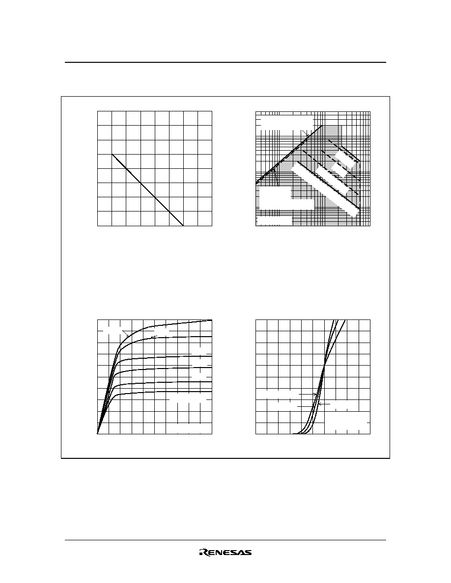
Main Characteristics
-500
-100
-200
-20
-50
-10
-2
-5
-1
-0.5
-0.3
-0.5
-1
-2
-5
-10 -20
-50 -100
Drain to Source Voltage V
DS
(V)
Drain Current I
D
(A)
Drain Current I
D
(A)
Drain Current I
D
(A)
Maximum Safe Operation Area
-50
-40
-30
-20
-10
0
-2
-4
-6
-8
-10
-10 V
V = -3.5 V
GS
Drain to Source Voltage V
DS
(V)
Typical Output Characteristics
0
-1
-2
-3
-4
-5
Tc = -25
∞
C
25
∞
C
75
∞
C
Gate to Source Voltage V
GS
(V)
Typical Transfer Characteristics
100
µ
s
1 ms
PW = 10 ms
DC Operation (Tc = 25
∞
C)
Ta = 25
∞
C
-20
-16
-12
-8
-4
-8 V
-6 V
-5 V
-4 V
Pulse Test
V = -10 V
DS
Pulse Test
80
60
40
20
0
50
100
150
200
Channel Dissipation Pch (W)
Case Temperature Tc (
∞
C)
Power vs. Temperature Derating
Thermal shut down
operation area
Operation
in this area
is limited by R
DS(on)

HAF1008(L), HAF1008(S)
Rev.1.00, May.13.2003, page 5 of 11
-1
-0.8
-0.6
-0.4
-0.2
0
-2
-4
-6
-8
-10
Pulse Test
Gate to Source Voltage V
GS
(V)
Drain to Source Saturation Voltage vs.
Gate to Source Voltage
Drain to Source Saturation Voltage
V
DS(on)
(V)
-0.1 -0.2
-0.5 -1
-2
-5
-10 -20
200
100
20
50
10
Drain Current I
D
(A)
Drain to Source On State Resistance
V
DS(on)
(m
)
Static Drain to Source Sate Resistance
vs. Drain Current
100
80
60
40
20
-25
0
25
50
75
100 125 150
0
Pulse Test
Case Temperature Tc (
∞
C)
Drain to Source On State Resistance
R
DS(on)
(m
)
Static Drain to Source on State Resistance
vs. Temperature
20
50
10
2
1
5
Drain Current I
D
(A)
Forward Transfer Admittance vs.
Drain Current
Forward Transfer Admittance |yfs| (S)
-5 A
I = -10 A
D
-50
V = -4 V
GS
-10 V
I = -10 A
D
-5 A
-10 A
-0.1 -0.2
-0.5 -1
-2
-5
-10 -20
-50
0.5
Tc = -25
∞
C
25
∞
C
75
∞
C
DS
V = -10 V
Pulse Test
V = -4 V
GS
-10 V
Pulse Test
-5 A