 | –≠–ª–µ–∫—Ç—Ä–æ–Ω–Ω—ã–π –∫–æ–º–ø–æ–Ω–µ–Ω—Ç: HAT2198R | –°–∫–∞—á–∞—Ç—å:  PDF PDF  ZIP ZIP |
Rev.2.00, Oct.18.2004, page 1 of 7
HAT2198R
Silicon N Channel Power MOS FET
Power Switching
REJ03G0062-0200
Rev.2.00
Oct.18.2004
Features
∑
High speed switching
∑
Capable of 4.5 V gate drive
∑
Low drive current
∑
High density mounting
∑
Low on-resistance
R
DS(on)
= 7.2 m
typ. (at V
GS
= 10 V)
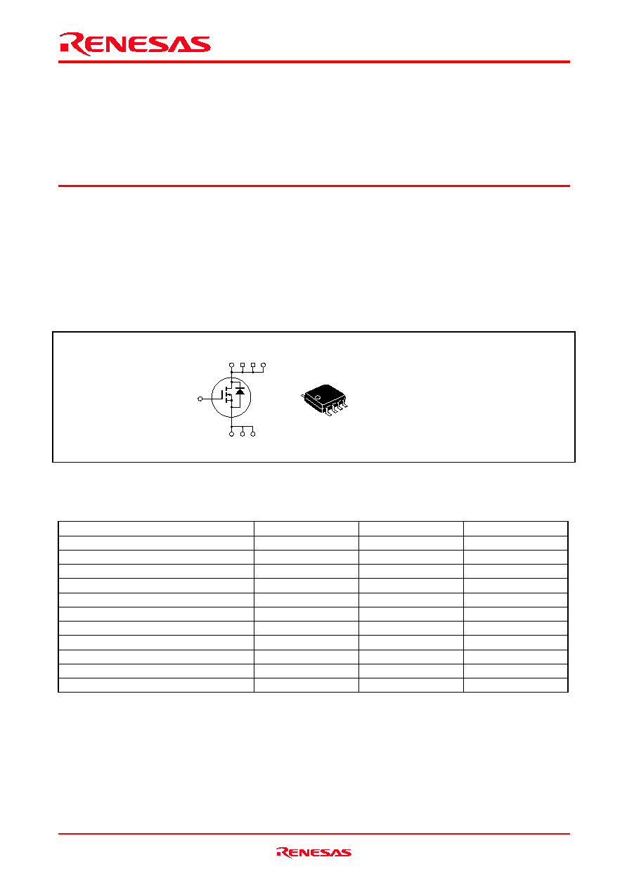
Outline
SOP-8
1 2
3
4
5
6
7
8
1, 2, 3 Source
4 Gate
5, 6, 7, 8 Drain
G
D
S S S
D D D
4
1 2
3
5
6 7 8
Absolute Maximum Ratings
(Ta = 25∞C)
Item
Symbol
Ratings
Unit
Drain to source voltage
V
DSS
30
V
Gate to source voltage
V
GSS
±20
V
Drain current
I
D
14
A
Drain peak current
I
D(pulse)
Note1
112
A
Body-drain diode reverse drain current
I
DR
14
A
Avalanche current
I
AP
Note 2
14
A
Avalanche energy
E
AR
Note 2
19.6
mJ
Channel dissipation
Pch
Note3
2.5
W
Channel to ambient thermal impedance
ch-a
Note3
50
∞
C/W
Channel temperature
Tch
150
∞
C
Storage temperature
Tstg
≠55 to +150
∞
C
Notes: 1. PW
10
µ
s, duty cycle
1%
2. Value at Tch = 25
∞
C, Rg
50
3. When using the glass epoxy board (FR4 40 x 40 x 1.6 mm), PW
10s

HAT2198R
Rev.2.00, Oct.18.2004, page 2 of 7
Electrical Characteristics
(Ta = 25∞C)
Item
Symbol
Min
Typ
Max
Unit
Test Conditions
Drain to source breakdown voltage
V
(BR)DSS
30
--
--
V
I
D
= 10 mA, V
GS
= 0
Gate to source leak current
I
GSS
--
--
± 0.1
µ
A
V
GS
= ±20 V, V
DS
= 0
Zero gate voltage drain current
I
DSS
--
--
1
µ
A
V
DS
= 30 V, V
GS
= 0
Gate to source cutoff voltage
V
GS(off)
1.0
--
2.5
V
V
DS
= 10 V,
I
D
= 1 mA
R
DS(on)
--
7.2
9.0
m
I
D
= 7 A, V
GS
= 10 V
Note4
Static drain to source on state
resistance
R
DS(on)
--
9.6
14.0
m
I
D
= 7 A, V
GS
= 4.5 V
Note4
Forward transfer admittance
|y
fs
|
18
30
--
S
I
D
= 7 A, V
DS
= 10 V
Note4
Input capacitance
Ciss
--
1650
--
pF
Output capacitance
Coss
--
390
--
pF
Reverse transfer capacitance
Crss
--
135
--
pF
V
DS
= 10 V
V
GS
= 0
f = 1 MHz
Gate Resistance
Rg
--
0.55
--
Total gate charge
Qg
--
11
--
nC
Gate to source charge
Qgs
--
4.7
--
nC
Gate to drain charge
Qgd
--
2.5
--
nC
V
DD
= 10 V
V
GS
= 4.5 V
I
D
= 14 A
Turn-on delay time
t
d(on)
--
8.5
--
ns
Rise time
t
r
--
5
--
ns
Turn-off delay time
t
d(off)
--
38
--
ns
Fall time
t
f
--
3.8
--
ns
V
GS
= 10 V, I
D
= 7 A
V
DD
10 V
R
L
= 1.42
Rg = 4.7
Body≠drain diode forward voltage
V
DF
--
0.80
1.04
V
IF = 14 A, V
GS
= 0
Note4
Body≠drain diode reverse recovery
time
t
rr
--
28
--
ns
IF = 14 A, V
GS
= 0
diF/ dt = 100 A/
µ
s
Notes: 4. Pulse test
HAT2198R
Rev.2.00, Oct.18.2004, page 3 of 7
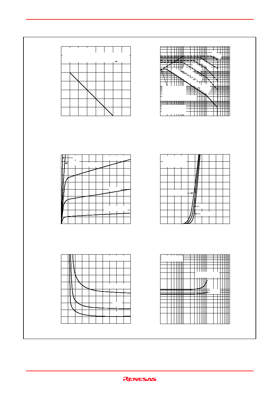
Main Characteristics
Channel Dissipation Pch (W)
Ambient Temperature Ta (∞C)
Power vs. Temperature Derating
4.0
3.0
2.0
1.0
0
50
100
150
200
Test Condition :
When using the glass epoxy board
(FR4 40 x 40 x 1.6 mm), PW < 10 s
Drain to Source Voltage V
DS
(V)
Drain Current I
D
(A)
Maximum Safe Operation Area
Note 5 :
When using the glass epoxy board
(FR4 40x40x1.6 mm)
100
10
1
0.1
0.01
0.1
0.3
1
3
10
30
100
500
Ta = 25
∞C
1 shot Pulse
PW = 10 m
s
10 µ
s
100
µs
Operation in
this area is
limited by R
DS(on)
Note 5
DC Operation
(PW < 10 s)
1 ms
Drain to Source Voltage V
DS
(V)
Drain Current I
D
(A)
Typical Output Characteristics
20
16
12
8
4
0
2
4
6
8
10
V
GS
= 2.4 V
10 V
3 V
Pulse Test
2.6 V
Gate to Source Voltage V
GS
(V)
Drain Current I
D
(A)
Typical Transfer Characteristics
20
16
12
8
4
0
1
2
3
4
5
Tc = 75
∞C
25
∞C
≠25
∞C
V
DS
= 10 V
Pulse Test
Gate to Source Voltage V
GS
(V)
Drain to Source Voltage V
DS(on)
(mV)
Drain to Source Saturation Voltage vs.
Gate to Source Voltage
300
240
180
120
60
0
4
8
12
16
20
Pulse Test
I
D
= 20 A
5 A
10 A
Drain Current I
D
(A)
Drain to Source On State Resistance
V
DS(on)
(m
)
Static Drain to Source on State Resistance
vs. Drain Current
20
10
2
5
1
1
10
100
1000
100
50
V = 4.5 V
GS
10 V
Pulse Test
2.8 V
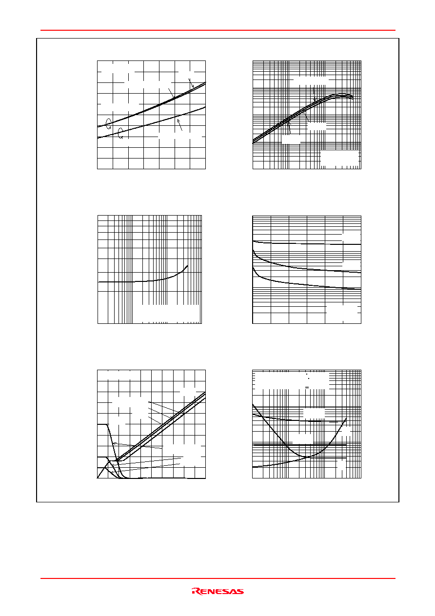
HAT2198R
Rev.2.00, Oct.18.2004, page 4 of 7
Crss
Case Temperature Tc (
∞C)
Static Drain to Source on State Resistance
Static Drain to Source on State Resistance
vs. Temperature
20
16
12
8
4
-25
0
50
25
100
75
125 150
0
R
DS(on)
(m
)
I
D
= 5 A, 10 A
5 A, 10 A, 20 A
V
GS
= 4.5 V
10 V
Pulse Test
Forward Transfer Admittance |yfs| (S)
Drain Current I
D
(A)
Forward Transfer Admittance vs.
Drain Current
3
30
0.1
1
10
100
0.3
10
100
1000
1
Tc = ≠25
∞C
V
DS
= 10 V
Pulse Test
75
∞C
25
∞C
Reverse Drain Current I
DR
(A)
Reverse Recovery Time trr (ns)
Body≠Drain Diode Reverse
Recovery Time
1
10
100
100
20
50
10
0.1
di/dt = 100 A/
µs
V
GS
= 0, Ta = 25
∞C
Capacitance C (pF)
Drain to Source Voltage V
DS
(V)
Typical Capacitance vs.
Drain to Source Voltage
0
10
5
15
20
25
30
10000
3000
1000
300
100
30
10
V
GS
= 0
f = 1 MHz
Gate Charge Qg (nc)
Drain to Source Voltage V
DS
(V)
Gate to Source Voltage V (V)
GS
Dynamic Input Characteristics
50
40
30
20
10
0
20
16
12
8
4
8
16
24
32
40
0
I
D
= 14 A
V
DD
= 25 V
10 V
5 V
V
DD
= 25 V
10 V
5 V
Drain Current I
D
(A)
Switching Time t (ns)
Switching Characteristics
100
10
1
1
10
0.1
100
1000
V
GS
= 10 V, V
DS
= 10 V
Rg = 4.7
, duty < 1 %
d(on)
t
d(off)
t
r
t
t f
Ciss
20 A
V
DS
V
GS
Coss
HAT2198R
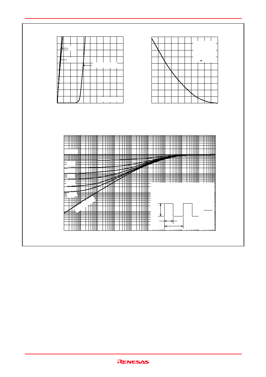
Rev.2.00, Oct.18.2004, page 5 of 7
Source to Drain Voltage V
SD
(V)
Reverse Drain Current I
DR
(A)
20
16
12
8
4
0
0.4
0.8
1.2
1.6
2.0
Reverse Drain Current vs.
Source to Drain Voltage
Pulse Test
5 V
V
GS
= 0,-5 V
10 V
20
16
12
8
4
25
50
75
100
125
150
0
Channel Temperature Tch (
∞C)
Repetitive Avalanche Energy E
AR
(mJ)
Maximum Avalanche Energy vs.
Channel Temperature Derating
I
AP
= 11 A
V
DD
= 15 V
duty < 0.1 %
Rg > 50
Pulse Width PW (s)
Normalized Transient Thermal Impedance vs. Pulse Width
Normalized Transient Thermal Impedance
s (t)
10
µ
100
µ
1 m
10 m
100 m
1
10
100
1000
10000
10
1
0.1
0.01
0.001
0.0001
1shot puls
e
DM
P
PW
T
D =
PW
T
ch - f(t) = s (t) x ch - f
ch - f = 83.3∞C/W, Ta = 25∞C
When using the glass epoxy board
(FR4 40 x 40 x 1.6 mm)
D = 1
0.5
0.2
0.1
0.05
0.02
0.01