Rev.1.00, Apr.17.2003, page 1 of 39
HD151TS205SS
Mother Board Clock Generator
for Intel P4+ Chipset (Springdale)
REJ03D0002≠0100Z
Preliminary
Rev.1.00
Apr.17.2003
Description
The HD151TS205SS is Intel CK409 type high-performance, low-skew, low-jitter, PC motherboard clock
generator. It is specifically designed for Intel Pentium
Æ
4+ chipset.
Features
∑
3 differential pairs of current mode control CPU clocks
∑
1 differential pair of Serial Reference Clock (SRC), selectable 100MHz/200MHz
∑
6 copies PCI clocks and 3 copies PCIF clocks @3.3V, 33.3MHz
∑
1 copy PCI clock @3.3V, selectable 33.3MHz/25MHz
∑
1 copy USB clock @3.3V, selectable 48MHz/24MHz
∑
1 copy DOT clock @3.3V, 48MHz
∑
4 copies of 3V66 clocks @3.3V, 66.6MHz
∑
1 copy of 3V66/VCH clock @3.3V, selectable 66.6MHz/48MHz
∑
2 copies of REF clocks @3.3V, 14.318MHz
∑
Power save and clock stop function
∑
I
2
C
TM
serial port programming
∑
Programmable Clock Control (Spread Spectrum Percentage, Clock Output Skew, Slew Rate)
∑
Watchdog timer and reset output
∑
56pin SSOP (300 mils)
Note: I
2
C is a trademark of Philips Corporation.
Pentium is registered trademark of Intel Corporation

HD151TS205SS
Rev.1.00, Apr.17.2003, page 2 of 39
Key Specifications
∑
Supply Voltages: VDD = 3.3 V±5%
∑
CPU clock cycle to cycle jitter = |125|ps (SSC Disabled)
∑
CPU clock group Skew = 100ps
∑
3V66 clock group Skew = 250psmax
∑
PCI clock group Skew = 500psmax
HD151TS205SS
Rev.1.00, Apr.17.2003, page 3 of 39
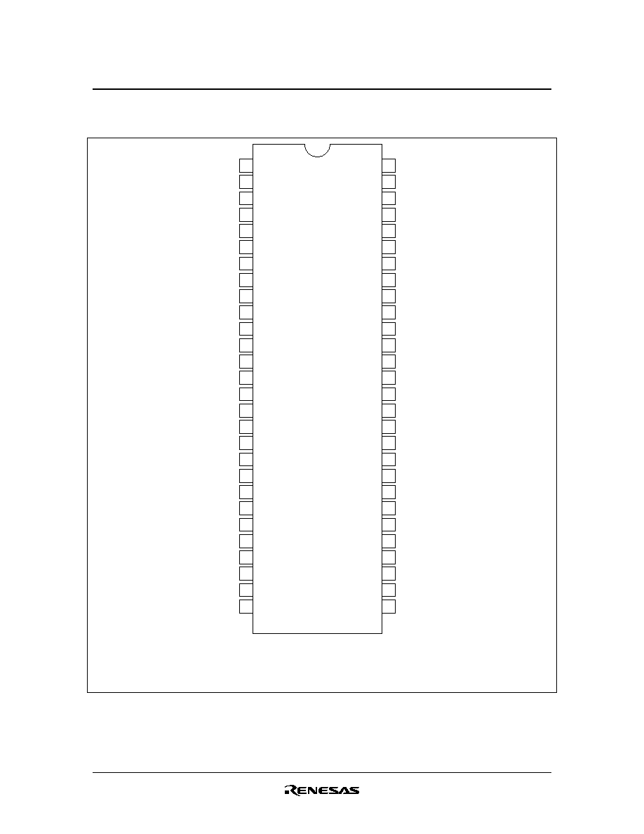
Pin Arrangement
1
2
3
4
5
6
7
8
9
10
REF0
REF1
VDD_REF
XTAL_IN
XTAL_OUT
VSS_REF
FS2/PCIF_0
FS4/PCIF_1
VDD_PCI
VSS_PCI
PCI_1
MODE/PCI_0
PCI_2
PCI_3
VDD_PCI
VSS_PCI
SEL100_200/PCI_4
SEL33_25/PCI_5
PCI_6
PWRDWN#/SAFE_F#
3V66_0/RESET#
3V66_1
VDD_3V66
PCIF_2
11
12
13
14
15
16
17
18
19
20
21
22
23
24
33
34
35
36
37
38
39
40
41
42
43
44
45
46
47
48
49
50
51
52
53
54
55
56
VSS_48
VDD_48
VTT_PWRGD#
SRC#
SRC
CPU_1
CPU_0#
CPU_0
VSS_CPU
CPU_2
VDD_CPU
PCI_STOP#
VSS_SRC
CPU_STOP#
FS_A
IREF
VSS_A
FS_B
VDD_A
VDD_SRC
VSS_3V66
3V66_2
3V66_3
SCLK
25
26
27
28
29
30
31
32
SEL66_48/3V66_4/VCH
SDATA
SEL48_24/USB_48
FS3/DOT_48
VDD_CPU
CPU_1#
CPU_2#
VSS_IREF
(Top view)
PCI_STOP#, CPUSTOP#, PWRDWN# = 150 k
Internal Pull-up
HD151TS205SS
Rev.1.00, Apr.17.2003, page 4 of 39
Pin Descriptions
Pin name
No.
Type
Description
VSS_A
54
Ground
Ground for PLL
VSS_CPU
45
Ground
Ground for outputs
VSS_IREF
53
Ground
Ground for current reference
VSS_SRC
39
Ground
Ground for outputs
VSS_3V66
25
Ground
Ground for outputs
VSS_PCI
11, 17
Ground
Ground for outputs
VSS_REF
6
Ground
Ground for outputs
VSS_48
33
Ground
Ground for outputs
VDD_A
55
Power
3.3 V Power Supply for PLL
VDD_CPU
42, 48
Power
3.3 V Power Supply for outputs
VDD_SRC
36
Power
3.3 V Power Supply for outputs
VDD_3V66
24
Power
3.3 V Power Supply for outputs
VDD_PCI
10, 16
Power
3.3 V Power Supply for outputs
VDD_REF
3
Power
3.3 V Power Supply for outputs
VDD_48
34
Power
3.3 V Power Supply for outputs
REF0
1
OUTPUT
3.3 V 14.318 MHz reference clock.
REF1
2
OUTPUT
3.3V 14.318 MHz reference clock.
XTAL_IN
4
INPUT
14.318 MHz XTAL input.
XTAL_OUT
5
OUTPUT
14.318 MHz XTAL output.
Don't connect when an external clock is applied at XTAL_IN.
FS2/PCIF_0
7
INPUT/
OUTPUT
Frequency select latch input pin.
/Free running PCI clock 3.3 V output.
FS4/PCIF_1
8
INPUT/
OUTPUT
Frequency select latch input pin.
/Free running PCI clock 3.3 V output.
PCIF_2
9
OUTPUT
Free running PCI clock 3.3 V output.
MODE/PCI_0*
2
12
INPUT/
OUTPUT
Function select latch input pin for pin22.
1 = Reset#, 0 = clock output.
/ PCI clock 3.3 V output.
PCI_1
13
OUTPUT
PCI clock 3.3 V outputs.
PCI_2
14
OUTPUT
PCI clock 3.3 V outputs.
PCI_3
15
OUTPUT
PCI clock 3.3 V outputs.
SEL100_200/
PCI_4*
2
18
INPUT/
OUTPUT
Latched select input for SRC output.
1 = 200 MHz, 0 = 100 MHz
/PCI clock 3.3 V output.
SEL33_25/PCI_5*
2
19
INPUT/
OUTPUT
Latched select input for PCI5 output.
1 = 25 MHz, 0 = 33 MHz
/PCI clock 3.3 V output.
PCI_6
20
OUTPUT
PCI clock 3.3 V outputs.

HD151TS205SS
Rev.1.00, Apr.17.2003, page 5 of 39
Pin Descriptions (cont.)
Pin name
No.
Type
Description
PWRDWN#/
SAFE_F#
21
INPUT
PULL-UP*
1
PWRDWN#/SAFE_F# selectable input.
Default is PWRDWN# input.
Byte15[5] = "1" : SAFE_F# input.
PWRDWN# is all clocks stop pin.
Asynchronous active "Low" input.
When asserted low, all output clocks are disabled.
SAFE_F# is active "Low" input.
When SAFE_F# is "Low", frequency mode is changed to the
predefined frequency mode.
3V66_0/RESET#
22
OUTPUT
3V66 / Watchdog RESET# selectable output.
Default is 3V66 output.
This signal is active low and selected by Mode latch input.
3V66_1
23
OUTPUT
3V66 clock 3.3 V outputs.
3V66_2
26
OUTPUT
3V66 clock 3.3 V outputs.
3V66_3
27
OUTPUT
3V66 clock 3.3 V outputs.
SCLK
28
INPUT
PULL-UP*
1
Clock input for I
2
C logic.
SEL66_48/
3V66_4/VCH*
2
29
INPUT/
OUTPUT
Latched select input for 3V66/VCH output 1 = 48 MHz,
0 = 66.66 MHz. /3V66 or VCH clock output.
SDATA
30
IN/OUTPUT
PULL-UP*
1
Data input for I
2
C logic.
SEL48_24/
USB_48*
2
31
INPUT/
OUTPUT
Latched select input for 48_24 MHz output
1 = 24 MHz, 0 = 48 MHz/24_48 MHz clock 3.3 V output.
FS3/DOT_48
32
INPUT/
OUTPUT
Frequency select latch input pin.
/DOT_48 clock 3.3 V output.
VTT_PWRGD#
35
INPUT
PULL-UP*
1
Qualifying input that latches FS_A and FS_B.
When asserted low, FS_A and FS_B are latched.
SRC#
37
OUTPUT
"Complementary" clock of Differential Serial Reference Clock.
SRC
38
OUTPUT
"True" clock of Differential Serial Reference Clock.
CPU_0#
40
OUTPUT
"Complementary" clock of differential CPU clock.
CPU_0
41
OUTPUT
"True" clock of differential CPU clock.
CPU_1#
43
OUTPUT
"Complementary" clock of differential CPU clock.
CPU_1
44
OUTPUT
"True" clock of differential CPU clock.
CPU_2#
46
OUTPUT
"Complementary" clock of differential CPU clock.
CPU_2
47
OUTPUT
"True" clock of differential CPU clock.
PCI_STOP#
49
INPUT
PULL-UP *
1
PCI clocks stop pin. Active "Low" input.
When asserted low, PCI[6:0] and SRC clocks are
synchronously disabled in low state.
Usually this pin does not give to effect PCIF[2:0] clock outputs.
CPU_STOP#
50
INPUT
PULL-UP*
1
CPU clocks stop pin. Active "Low" input.
When asserted low, CPU[2:0] clocks are synchronously
disabled in high state and CPU#[2:0] clocks are synchronously
disabled in a low state.
FS_A
51
INPUT
CPU clocks frequency select latch input.
IREF
52
INPUT
A precision resistor is attached to this pin which is connected
to internal current reference.
A resistor is connected between this pin and GNDIREF.
FS_B
56
INPUT
CPU clocks frequency select latch input that is 3level input.
Note:
1. Those pins are 150k
internal pulled-UP.
2. Those pins are 150k
internal pulled-DOWN