
Rev.2.00, Jul.16.2004, page 1 of 7
HD26LS32A
Quadruple Differential Line Receivers With 3 State Outputs
REJ03D0296≠0200Z
(Previous ADE-205-578 (Z))
Rev.2.00
Jul.16.2004
Description
The HD26LS32A features quadruple line receivers designed to meet the specs of EIA standard RS-422A and RS-423.
This device operates from a single 5 V power supply. The enable function is common to all four receivers and offers a
choice of active high or active low input. Fail safe design ensures that if the inputs are open, the outputs will always be
high.
Features
∑
Ordering Information
Part Name
Package Type
Package Code
Package
Abbreviation
Taping Abbreviation
(Quantity)
HD26LS32AP
DILP-16 pin (JEITA) DP-16E, -16FV
P
--
Logic Diagram
1A
Enable G
Enable G
1Y
2Y
3Y
4Y
1B
2A
2B
3A
3B
4A
4B

HD26LS32A
Rev.2.00, Jul.16.2004, page 2 of 7
Pin Arrangement
(Top view)
1
2
3
4
5
6
7
1B
GND
1A
1Y
2Y
8
Enable G
2A
2B
13
14
15
10
11
12
9
16 V
CC
4B
4A
4Y
Enable G
3Y
3A
3B
Function Table
Differential Input
Enable
Output
A ≠ B
G
G
G
G
G
Y
V
ID
V
TH
H
X
H
X
L
H
V
TL
< V
ID
< V
TH
H
X
?
X
L
?
V
ID
V
TL
H
X
L
X
L
L
X
L
H
Z
H :
High level
L :
Low level
X :
Immaterial
? :
Irrelevant
Z :
High impedance
Absolute Maximum Ratings
Item
Symbol
Ratings
Unit
Supply Voltage
V
CC
*
1
7.0
V
Input Voltage A or B
V
IN
±25
V
Differential Input Voltage
V
ID
*
2
±25
V
Enable Input Voltage
V
IN
7
V
Output Sink Current
Iout
50
mA
Continuous Total Dissipation
P
T
1
W
Operating Temperature
Topr
0 to +70
∞C
Storage Temperature
Tstg
≠65 to 150
∞C
Notes: 1. All voltage values except for differential input voltage are with respect to network ground terminal.
2. Differential input voltage is measured at the noninverting input with respect to the corresponding inverting
input.
3. The absolute maximum ratings are values which must not individually be exceeded, and furthermore, no two
of which may be realized at the same time.

HD26LS32A
Rev.2.00, Jul.16.2004, page 3 of 7
Recommended Operating Conditions
Item
Symbol
Min
Typ
Max
Unit
Supply Voltage
V
CC
4.75
5.00
5.25
V
In Phase Input Voltage
V
IC
--
--
±7.0
V
Output Current
I
OH
--
--
≠440
µA
I
OL
--
--
8
mA
Operating Temperature
Topr
0
--
70
∞C
Electrical Characteristics
(Ta = 0 to +70∞C)
Item
Symbol Min Typ
*
1
Max Unit
Conditions
Differential Input High
Threshold Voltage
V
TH
--
--
0.2
V
V
IC
= ≠7 to +7 V V
OH
= 2.7V, I
OH
= ≠440 µA
Differential Input Low
V
TL
--
--
≠0.2
V
OL
= 0.4 V, I
OL
= 4 mA
Threshold Voltage
--
--
≠0.2
V
OL
= 0.45 V, I
OL
= 8 mA
Input Hysteresis*
2
V
TH
≠ V
TL
--
50
--
mV
Enable Input Voltage
V
IH
2.0
--
--
V
V
IL
--
--
0.8
Enable Input Clamp
Voltage
V
IK
--
--
≠1.5
V
CC
= 4.75 V, I
IN
= ≠18 mA
Output Voltage
V
OH
2.7
--
--
V
CC
= 4.75 V
V
ID
= 1 V, I
OH
= ≠440 µA
V
OL
--
--
0.4
V
IL
(
G) = 0.8 V
V
ID
= ≠1 V, I
OL
= 4 mA
--
--
0.45
V
ID
= ≠1 V, I
OL
= 8 mA
Off State (High
I
OZ
--
--
20
µA
V
CC
= 5.25 V
V
O
= 2.4 V
Impedance) Output
Current
--
--
≠20
V
O
= 0.4 V
Line Input Current
II
--
--
--
--
1.2
≠1.7
mA
V
I
= 15 V, Other Inputs ≠10 to +15 V
V
I
= ≠15 V, Other Inputs ≠15 to +10 V
Enable Input Current
I
I
(EN)
--
--
100
µA
V
I
= 5.5 V
I
IH
--
--
20
V
I
= 2.7 V
I
IL
--
--
≠0.36 mA
V
I
= 0.4 V
Input Resistance
ri
12
15
--
k
V
IC
= ≠15 to +15 V (Other Inputs AC GND)
Short Circuit Output
Current
I
OS
*
3
≠15
--
≠85
mA
V
CC
= 5.25 V
Supply Current
I
CC
--
52
70
V
CC
= 5.25 V, V
I
= 0 V (All Outputs Disable)
Notes: 1. All typical values are at V
CC
= 5 V, Ta = 25∞C,V
IC
= 0.
2. Hysteresis is the differential between the positive going input threshold voltage and the negative going input
threshold voltage.
3. Not more than one output should be shorted at a time.
Switching Characteristics
(V
CC
= 5 V, Ta = 25∞C)
Item
Symbol
Min
Typ
Max
Unit
Conditions
Propagation Delay Time
t
PLH
--
20
35
ns
C
L
= 15 pF
t
PHL
--
22
35
Output Enable Time
t
ZH
--
17
22
ns
C
L
= 15 pF
t
ZL
--
20
25
Output Disable Time
t
HZ
--
21
30
ns
C
L
= 5 pF
t
LZ
--
30
40

HD26LS32A
Rev.2.00, Jul.16.2004, page 4 of 7
1. t
PLH
, t
PHL
Test circuit
Pulse
Generator
Input
C
L
Output
2 k
V
CC
5 k
2 V
Waveforms
Input A
0 V
0 V
0 V
0 V
t
PLH
OH
V
OL
V
1.3 V
2.5 V
≠2.5 V
2.5 V
≠2.5 V
t
PHL
1.3 V
Input B
Output
HD26LS32A
Rev.2.00, Jul.16.2004, page 5 of 7
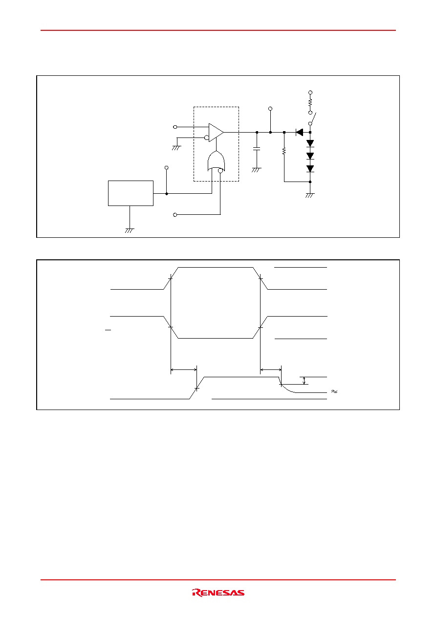
2. t
HZ
, t
ZH
Test circuit
Input
2.5 V
2 V
C
L
Output
2 k
V
CC
5 k
S1
Pulse
Generator
Waveforms
Enable G
1.3 V
1.3 V
1.3 V
1.3 V
t
ZH
OH
V
1.3 V
3 V
0 V
3 V
0 V
t
HZ
0.5 V
Output
Enable G
S1 : Open
0 V
1.4 V
S1 : Closed