Rev.6.00, Sep.01.2003, page 1 of 11
HD74LV1G86A
2≠input Exclusive≠OR Gate
REJ03D0070≠0600Z
(Previous ADE-205-322D (Z))
Rev.6.00
Sep.01.2003
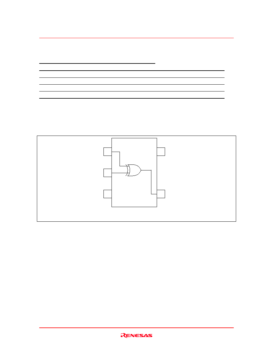
Description
The HD74LV1G86A performs the Boolean functions Y = A
B or Y =
AB + AB in positive logic. A
common application is as a true / complement element. If one of the inputs is low, the other input will be
reproduced in true form at the output. If one of the inputs is high, the signal on the other input will be
reproduced inverted form at the output. Low voltage and high-speed operation is suitable for the battery
powered products (e.g., notebook computers), and the low power consumption extends the battery life.
Features
∑
The basic gate function is lined up as Renesas uni logic series.
∑
Supplied on emboss taping for high-speed automatic mounting.
∑
Electrical characteristics equivalent to the HD74LV86A
Supply voltage range : 1.65 to 5.5 V
Operating temperature range : ≠40 to +85∞C
∑
All inputs V
IH
(Max.) = 5.5 V (@V
CC
= 0 V to 5.5 V)
All outputs V
O
(Max.) = 5.5 V (@V
CC
= 0 V)
∑
Output current ±6 mA (@V
CC
= 3.0 V to 3.6 V), ±12 mA (@V
CC
= 4.5 V to 5.5 V)
∑
All the logical input has hysteresis voltage for the slow transition.
∑
Ordering Information
Part Name
Package Type
Package Code
Package
Abbreviation
Taping Abbreviation
(Quantity)
CMPAK≠5V
HD74LV1G86ACME CMPAK≠5 pin
CMPAK≠5V(O)
CM
HD74LV1G86AVSE VSON≠5 pin
TNP≠5DV
VS
E (3,000 pcs/reel)
Note: Please consult the sales office for the above package availability.

HD74LV1G86A
Rev.6.00, Sep.01.2003, page 2 of 11
Outline and Article Indication
∑ HD74LV1G86A
Marking
= Control code
L 8
Index band
CMPAK≠5
∑
HD74LV1G86A
Marking
= Control code
L 8
VSON≠5
HD74LV1G86A
Rev.6.00, Sep.01.2003, page 3 of 11
Function Table
Inputs
A
B
Output Y
L
L
L
L
H
H
H
L
H
H
H
L
H : High level
L : Low level
Pin Arrangement
(Top view)
5
4
V
CC
1
2
3
IN B
IN A
GND
OUT Y

HD74LV1G86A
Rev.6.00, Sep.01.2003, page 4 of 11
Absolute Maximum Ratings
Item
Symbol
Ratings
Unit
Test Conditions
Supply voltage range
V
CC
≠0.5 to 7.0
V
Input voltage range
*1
V
I
≠0.5 to 7.0
V
≠0.5 to V
CC
+ 0.5
Output : H or L
Output voltage range
*1, 2
V
O
≠0.5 to 7.0
V
V
CC
: OFF
Input clamp current
I
IK
≠20
mA
V
I
< 0
Output clamp current
I
OK
±50
mA
V
O
< 0 or V
O
> V
CC
Continuous output current
I
O
±25
mA
V
O
= 0 to V
CC
Continuous current through
V
CC
or GND
I
CC
or I
GND
±50
mA
Maximum power dissipation
at Ta = 25∞C (in still air)
*3
P
T
200
mW
Storage temperature
Tstg
≠65 to 150
∞C
Notes:
The absolute maximum ratings are values, which must not individually be exceeded, and
furthermore no two of which may be realized at the same time.
1. The input and output voltage ratings may be exceeded if the input and output clamp-current
ratings are observed.
2. This value is limited to 5.5 V maximum.
3. The maximum package power dissipation was calculated using a junction temperature of 150∞C.

HD74LV1G86A
Rev.6.00, Sep.01.2003, page 5 of 11
Recommended Operating Conditions
Item
Symbol
Min
Max
Unit
Conditions
Supply voltage range
V
CC
1.65
5.5
V
Input voltage range
V
I
0
5.5
V
Output voltage range
V
O
0
V
CC
V
--
1
V
CC
= 1.65 to 1.95 V
--
2
V
CC
= 2.3 to 2.7 V
--
6
V
CC
= 3.0 to 3.6 V
I
OL
--
12
V
CC
= 4.5 to 5.5 V
--
≠1
V
CC
= 1.65 to 1.95 V
--
≠2
V
CC
= 2.3 to 2.7 V
--
≠6
V
CC
= 3.0 to 3.6 V
Output current
I
OH
--
≠12
mA
V
CC
= 4.5 to 5.5 V
0
300
V
CC
= 1.65 to 1.95 V
0
200
V
CC
= 2.3 to 2.7 V
0
100
V
CC
= 3.0 to 3.6 V
Input transition rise or fall rate
t /
v
0
20
ns / V
V
CC
= 4.5 to 5.5 V
Operating free-air temperature T
a
≠40
85
∞C
Note: Unused or floating inputs must be held high or low.