
Regarding the change of names mentioned in the document, such as Hitachi
Electric and Hitachi XX, to Renesas Technology Corp.
The semiconductor operations of Mitsubishi Electric and Hitachi were transferred to Renesas
Technology Corporation on April 1st 2003. These operations include microcomputer, logic, analog
and discrete devices, and memory chips other than DRAMs (flash memory, SRAMs etc.)
Accordingly, although Hitachi, Hitachi, Ltd., Hitachi Semiconductors, and other Hitachi brand
names are mentioned in the document, these names have in fact all been changed to Renesas
Technology Corp. Thank you for your understanding. Except for our corporate trademark, logo and
corporate statement, no changes whatsoever have been made to the contents of the document, and
these changes do not constitute any alteration to the contents of the document itself.
Renesas Technology Home Page: http://www.renesas.com
Renesas Technology Corp.
Customer Support Dept.
April 1, 2003
To all our customers

Cautions
Keep safety first in your circuit designs!
1. Renesas Technology Corporation puts the maximum effort into making semiconductor products better
and more reliable, but there is always the possibility that trouble may occur with them. Trouble with
semiconductors may lead to personal injury, fire or property damage.
Remember to give due consideration to safety when making your circuit designs, with appropriate
measures such as (i) placement of substitutive, auxiliary circuits, (ii) use of nonflammable material or
(iii) prevention against any malfunction or mishap.
Notes regarding these materials
1. These materials are intended as a reference to assist our customers in the selection of the Renesas
Technology Corporation product best suited to the customer's application; they do not convey any
license under any intellectual property rights, or any other rights, belonging to Renesas Technology
Corporation or a third party.
2. Renesas Technology Corporation assumes no responsibility for any damage, or infringement of any
third-party's rights, originating in the use of any product data, diagrams, charts, programs, algorithms, or
circuit application examples contained in these materials.
3. All information contained in these materials, including product data, diagrams, charts, programs and
algorithms represents information on products at the time of publication of these materials, and are
subject to change by Renesas Technology Corporation without notice due to product improvements or
other reasons. It is therefore recommended that customers contact Renesas Technology Corporation
or an authorized Renesas Technology Corporation product distributor for the latest product information
before purchasing a product listed herein.
The information described here may contain technical inaccuracies or typographical errors.
Renesas Technology Corporation assumes no responsibility for any damage, liability, or other loss
rising from these inaccuracies or errors.
Please also pay attention to information published by Renesas Technology Corporation by various
means, including the Renesas Technology Corporation Semiconductor home page
(http://www.renesas.com).
4. When using any or all of the information contained in these materials, including product data, diagrams,
charts, programs, and algorithms, please be sure to evaluate all information as a total system before
making a final decision on the applicability of the information and products. Renesas Technology
Corporation assumes no responsibility for any damage, liability or other loss resulting from the
information contained herein.
5. Renesas Technology Corporation semiconductors are not designed or manufactured for use in a device
or system that is used under circumstances in which human life is potentially at stake. Please contact
Renesas Technology Corporation or an authorized Renesas Technology Corporation product distributor
when considering the use of a product contained herein for any specific purposes, such as apparatus or
systems for transportation, vehicular, medical, aerospace, nuclear, or undersea repeater use.
6. The prior written approval of Renesas Technology Corporation is necessary to reprint or reproduce in
whole or in part these materials.
7. If these products or technologies are subject to the Japanese export control restrictions, they must be
exported under a license from the Japanese government and cannot be imported into a country other
than the approved destination.
Any diversion or reexport contrary to the export control laws and regulations of Japan and/or the
country of destination is prohibited.
8. Please contact Renesas Technology Corporation for further details on these materials or the products
contained therein.

HD74LV1GW57A
Configurable Multiple≠Function Gate
ADE-205-717 (Z)
Rev.0
Feb. 2003
Description
The HD74LV1GW57A has configurable multiple≠function gate in a 6 pin package. The Output state is
determined by eight patterns of 3≠bit input. The user can choose the logic functions AND, NAND, NOR,
EX≠NOR. Low voltage and high speed operation is suitable for the battery powered products (e.g.,
notebook computers), and the low power consumption extends the battery life.
Features
∑
The basic gate function is lined up as hitachi uni logic series.
∑
Supplied on emboss taping for high speed automatic mounting.
∑
Supply voltage range : 1.65 to 5.5 V
Operating temperature range : ≠40 to +85∞C
∑
All inputs V
IH
(Max.) = 5.5 V (@V
CC
= 0 V to 5.5 V)
All outputs V
O
(Max.) = 5.5 V (@V
CC
= 0 V)
∑
Output current ±6 mA (@V
CC
= 3.0 V to 3.6 V), ±12 mA (@V
CC
= 4.5 V to 5.5 V)
∑
All the logical input has hysteresis voltage for the slow transition.
∑
Ordering Information
Part Name
Package Type
Package Code
Package
Abbreviation
Taping
Abbreviation (Quantity)
HD74LV1GW57ACME
CMPAK-6 pin
CMPAK-6V(O)
CM
E (3,000 pcs / Reel)

HD74LV1GW57A
Rev.0, Feb. 2003, page 2 of 11
Outline and Article Indication
∑ HD74LV1GW57A
Marking
= Control code
W R
Index band
CMPAK≠6
Function Table
Inputs
Output
IN2
IN1
IN0
Y
L
L
L
H
L
L
H
L
L
H
L
H
L
H
H
L
H
L
L
L
H
L
H
L
H
H
L
H
H
H
H
H
H : High level
L : Low level
HD74LV1GW57A
Rev.0, Feb. 2003, page 3 of 11
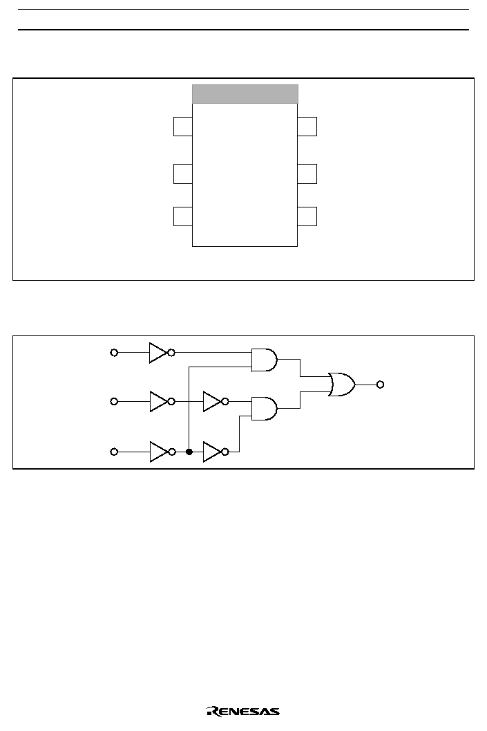
Pin Arrangement
(Top view)
V
CC
2
5
GND
6
IN2
1
IN1
3
IN0
4
Y
Logic Diagram
IN0
IN1
IN2
Y
HD74LV1GW57A
Rev.0, Feb. 2003, page 4 of 11
Function Selection Table
Logic Function
Figure No.
2≠input AND
1
2≠input AND with both inputs inverted
4
2≠input NAND with one input inverted
2, 3
2≠input OR with one input inverted
2, 3
2≠input NOR
4
2≠input NOR with both inputs inverted
1
2≠input EX≠NOR
5
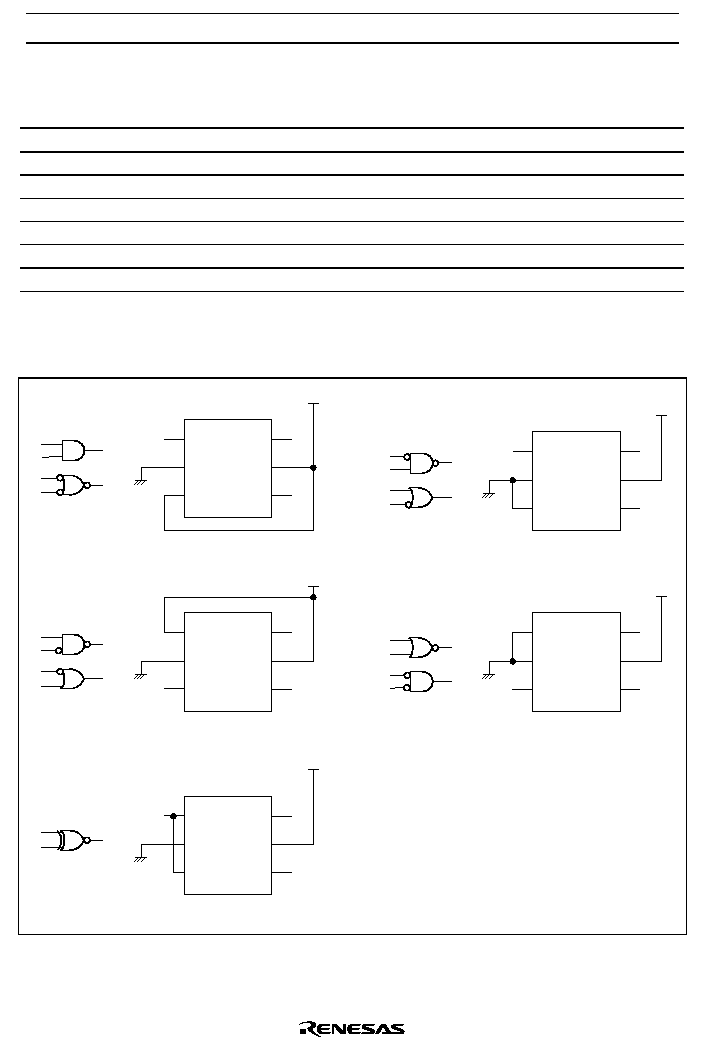
Logic Configurations
Y
Y
A
A
B
A
B
1 (IN1)
(IN2) 6
2 (GND) (V
CC
) 5
3 (IN0)
(Y) 4
B
V
CC
Y
Y
Y
A
A
B
A
B
1 (IN1)
(IN2) 6
2 (GND) (V
CC
) 5
3 (IN0)
(Y) 4
B
V
CC
Y
Figure 1. 2≠inputs AND Gate
Y
Y
A
A
B
A
B
1 (IN1)
(IN2) 6
2 (GND) (V
CC
) 5
3 (IN0)
(Y) 4
B
V
CC
Y
Figure 2. 2≠inputs NAND Gate
with A input inverted
Figure 4. 2≠inputs NOR Gate
Figure 3. 2≠inputs NAND Gate
with B input inverted
Y
A
A
B
1 (IN1)
(IN2) 6
2 (GND) (V
CC
) 5
3 (IN0)
(Y) 4
B
V
CC
Y
Figure 5. 2≠inputs EX≠NOR Gate
Y
Y
A
A
B
A
B
1 (IN1)
(IN2) 6
2 (GND) (V
CC
) 5
3 (IN0)
(Y) 4
B
V
CC
Y
HD74LV1GW57A
Rev.0, Feb. 2003, page 5 of 11
Absolute Maximum Ratings
Item
Symbol
Ratings
Unit
Test Conditions
Supply voltage range
V
CC
≠0.5 to 7.0
V
Input voltage range
*1
V
I
≠0.5 to 7.0
V
≠0.5 to V
CC
+ 0.5
Output : H or L
Output voltage range
*1, 2
V
O
≠0.5 to 7.0
V
V
CC
: OFF
Input clamp current
I
IK
≠20
mA
V
I
< 0
Output clamp current
I
OK
±50
mA
V
O
< 0 or V
O
> V
CC
Continuous output current
I
O
±25
mA
V
O
= 0 to V
CC
Continuous current through
V
CC
or GND
I
CC
or I
GND
±50
mA
Maximum power dissipation
at Ta = 25∞C (in still air)
*3
P
T
200
mW
Storage temperature
Tstg
≠65 to 150
∞C
Notes:
The absolute maximum ratings are values which must not individually be exceeded, and
furthermore no two of which may be realized at the same time.
1. The input and output voltage ratings may be exceeded if the input and output clamp-current
ratings are observed.
2. This value is limited to 5.5 V maximum.
3. The maximum package power dissipation was calculated using a junction temperature of 150∞C.
HD74LV1GW57A
Rev.0, Feb. 2003, page 6 of 11
Recommended Operating Conditions
Item
Symbol
Min
Max
Unit
Conditions
Supply voltage range
V
CC
1.65
5.5
V
Input voltage range
V
I
0
5.5
V
Output voltage range
V
O
0
V
CC
V
--
1
V
CC
= 1.65 to 1.95 V
--
2
V
CC
= 2.3 to 2.7 V
--
6
V
CC
= 3.0 to 3.6 V
I
OL
--
12
V
CC
= 4.5 to 5.5 V
--
≠1
V
CC
= 1.65 to 1.95 V
--
≠2
V
CC
= 2.3 to 2.7 V
--
≠6
V
CC
= 3.0 to 3.6 V
Output current
I
OH
--
≠12
mA
V
CC
= 4.5 to 5.5 V
0
300
V
CC
= 1.65 to 1.95 V
0
200
V
CC
= 2.3 to 2.7 V
0
100
V
CC
= 3.0 to 3.6 V
Input transition rise or fall rate
t /
v
0
20
ns / V
V
CC
= 4.5 to 5.5 V
Operating free-air temperature T
a
≠40
85
∞C
Note: Unused or floating inputs must be held high or low.
HD74LV1GW57A
Rev.0, Feb. 2003, page 7 of 11
Electrical Characteristic
∑
Ta = ≠40 to 85∞C
Item
Symbol V
CC
(V) *
Min
Typ
Max
Unit
Test condition
1.65 to 1.95 --
--
V
CC
◊
0.75
2.5
--
--
1.75
3.3
--
--
2.31
V
T
+
5.0
--
--
3.50
1.65 to 1.95 V
CC
◊
0.25 --
--
2.5
0.75
--
--
3.3
0.99
--
--
V
T
≠
5.0
1.5
--
--
1.65 to 1.95 0.1
--
V
CC
◊
0.4
2.5
0.25
--
1.0
3.3
0.33
--
1.32
Threshold
voltage
V
T
5.0
0.5
--
2.0
V
Min to Max V
CC
≠0.1
--
--
I
OH
= ≠50
µ
A
1.65
1.4
--
--
I
OH
= ≠1 mA
2.3
2.0
--
--
I
OH
= ≠2 mA
3.0
2.48
--
--
I
OH
= ≠6 mA
V
OH
4.5
3.8
--
--
I
OH
= ≠12 mA
Min to Max --
--
0.1
I
OL
= 50
µ
A
1.65
--
--
0.3
I
OL
= 1 mA
2.3
--
--
0.4
I
OL
= 2 mA
3.0
--
--
0.44
I
OL
= 6 mA
Output voltage
V
OL
4.5
--
--
0.55
V
I
OL
= 12 mA
Input current
I
IN
0 to 5.5
--
--
±1
µ
A
V
IN
= 5.5 V or GND
Quiescent
supply current
I
CC
5.5
--
--
10
µ
A
V
IN
= V
CC
or GND,
I
O
= 0
Output leakage
current
I
OFF
0
--
--
5
µ
A
V
IN
or V
O
= 0 to 5.5
V
Input capacitance C
IN
3.3
--
3.0
--
pF
V
IN
= V
CC
or GND
Note: For conditions shown as Min or Max, use the appropriate values under recommended operating
conditions.

HD74LV1GW57A
Rev.0, Feb. 2003, page 8 of 11
Switching Characteristics
∑
V
CC
= 1.8±0.15 V
Ta = 25∞C
Ta = ≠40 to 85∞C
Item
Symbol
Min
Typ
Max
Min
Max
Unit Test
Conditions
FROM
(Input)
TO
(Output)
--
15.8
29.4
1.0
33.0
C
L
= 15 pF
Propagation
delay time
t
PLH
t
PHL
--
22.6
40.9
1.0
45.0
ns
C
L
= 50 pF
IN
Y
∑
V
CC
= 2.5±0.2 V
Ta = 25∞C
Ta = ≠40 to 85∞C
Item
Symbol
Min
Typ
Max
Min
Max
Unit Test
Conditions
FROM
(Input)
TO
(Output)
--
9.4
17.6
1.0
21.0
C
L
= 15 pF
Propagation
delay time
t
PLH
t
PHL
--
12.6
22.6
1.0
26.5
ns
C
L
= 50 pF
IN
Y
∑
V
CC
= 3.3±0.3 V
Ta = 25∞C
Ta = ≠40 to 85∞C
Item
Symbol
Min
Typ
Max
Min
Max
Unit Test
Conditions
FROM
(Input)
TO
(Output)
--
7.0
11.0
1.0
13.0
C
L
= 15 pF
Propagation
delay time
t
PLH
t
PHL
--
9.5
14.5
1.0
16.5
ns
C
L
= 50 pF
IN
Y
∑
V
CC
= 5.0±0.5 V
Ta = 25∞C
Ta = ≠40 to 85∞C
Item
Symbol
Min
Typ
Max
Min
Max
Unit Test
Conditions
FROM
(Input)
TO
(Output)
--
4.8
6.8
1.0
8.0
C
L
= 15 pF
Propagation
delay time
t
PLH
t
PHL
--
6.3
8.8
1.0
10.0
ns
C
L
= 50 pF
IN
Y
Operating Characteristics
∑
C
L
= 50 pF
Ta = 25∞C
Item
Symbol
V
CC
(V)
Min
Typ
Max
Unit
Test Conditions
3.3
--
8.5
--
Power dissipation
capacitance
C
PD
5.0
--
10.0
--
pF
f = 10 MHz

HD74LV1GW57A
Rev.0, Feb. 2003, page 9 of 11
Test Circuit
C
L
Measurement point
Note: C
L
includes probe and jig capacitance.
*
Input
In phase output
90%
50%
10%
t
PLH
t
PHL
V
CC
GND
V
OH
V
OL
t
PHL
t
PLH
90%
50%
10%
50%
50%
50%
50%
∑
Waveforms
Out of phase output
V
OH
V
OL
Notes: 1. Input waveform : PRR
1 MHz, Zo = 50
, t
r
3 ns, t
f
3 ns.
2. The output are measured one at a time with one transition per measurement.
t
r
t
f
HD74LV1GW57A
Rev.0, Feb. 2003, page 10 of 11
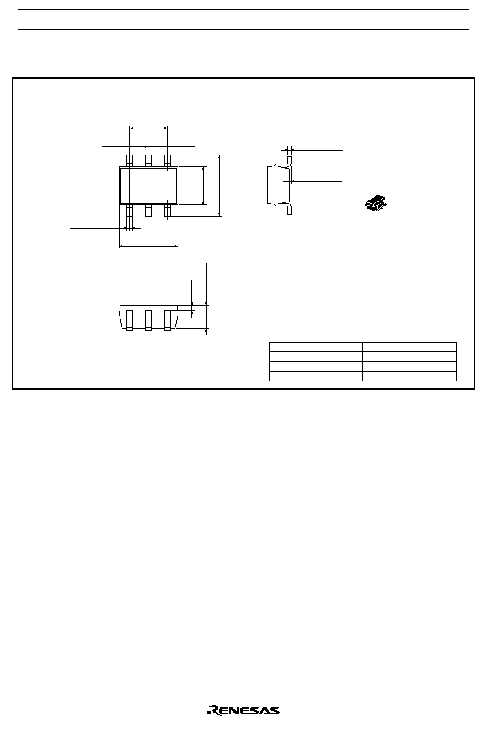
Package Dimensions
0.15 ± 0.05
2.0 ± 0.1*
(0.1)
+ 0.1
≠ 0.05
Hitachi Code
JEDEC
JEITA
Mass (reference value)
CMPAK-6V(O)
--
Conforms
0.006 g
Unit: mm
1.3 ± 0.05*
(2.1)
6 ≠ 0.2
+ 0.02 ≠ 0.03
0.88
(0.65)
(0.65)
(1.3)
0.025 ≠ 0.1
* Sn-Bi plating.
** The value does not include Resin Bar.
(One side: 0.15 mm (max))

HD74LV1GW57A
Rev.0, Feb. 2003, page 11 of 11
Disclaimer
1. Hitachi neither warrants nor grants licenses of any rights of Hitachi's or any third party's patent,
copyright, trademark, or other intellectual property rights for information contained in this document.
Hitachi bears no responsibility for problems that may arise with third party's rights, including
intellectual property rights, in connection with use of the information contained in this document.
2. Products and product specifications may be subject to change without notice. Confirm that you have
received the latest product standards or specifications before final design, purchase or use.
3. Hitachi makes every attempt to ensure that its products are of high quality and reliability. However,
contact Hitachi's sales office before using the product in an application that demands especially high
quality and reliability or where its failure or malfunction may directly threaten human life or cause risk
of bodily injury, such as aerospace, aeronautics, nuclear power, combustion control, transportation,
traffic, safety equipment or medical equipment for life support.
4. Design your application so that the product is used within the ranges guaranteed by Hitachi particularly
for maximum rating, operating supply voltage range, heat radiation characteristics, installation
conditions and other characteristics. Hitachi bears no responsibility for failure or damage when used
beyond the guaranteed ranges. Even within the guaranteed ranges, consider normally foreseeable
failure rates or failure modes in semiconductor devices and employ systemic measures such as fail-
safes, so that the equipment incorporating Hitachi product does not cause bodily injury, fire or other
consequential damage due to operation of the Hitachi product.
5. This product is not designed to be radiation resistant.
6. No one is permitted to reproduce or duplicate, in any form, the whole or part of this document without
written approval from Hitachi.
7. Contact Hitachi's sales office for any questions regarding this document or Hitachi semiconductor
products.
Sales Offices
Hitachi, Ltd.
Semiconductor & Integrated Circuits
Nippon Bldg., 2-6-2, Ohte-machi, Chiyoda-ku, Tokyo 100-0004, Japan
Tel: (03) 3270-2111 Fax: (03) 3270-5109
Copyright © Hitachi, Ltd., 2003. All rights reserved. Printed in Japan.
Hitachi Asia Ltd.
Hitachi Tower
16 Collyer Quay #20-00
Singapore 049318
Tel : <65>-6538-6533/6538-8577
Fax : <65>-6538-6933/6538-3877
URL : http://semiconductor.hitachi.com.sg
URL
http://www.hitachisemiconductor.com/
Hitachi Asia Ltd.
(Taipei Branch Office)
4/F, No. 167, Tun Hwa North Road
Hung-Kuo Building
Taipei (105), Taiwan
Tel : <886>-(2)-2718-3666
Fax : <886>-(2)-2718-8180
Telex : 23222 HAS-TP
URL : http://semiconductor.hitachi.com.tw
Hitachi Asia (Hong Kong) Ltd.
Group III (Electronic Components)
7/F., North Tower
World Finance Centre,
Harbour City, Canton Road
Tsim Sha Tsui, Kowloon Hong Kong
Tel : <852>-2735-9218
Fax : <852>-2730-0281
URL : http://semiconductor.hitachi.com.hk
Hitachi Europe GmbH
Electronic Components Group
Dornacher Str 3
D-85622 Feldkirchen
Postfach 201, D-85619 Feldkirchen
Germany
Tel: <49> (89) 9 9180-0
Fax: <49> (89) 9 29 30 00
Hitachi Europe Ltd.
Electronic Components Group
Whitebrook Park
Lower Cookham Road
Maidenhead
Berkshire SL6 8YA, United Kingdom
Tel: <44> (1628) 585000
Fax: <44> (1628) 778322
Hitachi Semiconductor
(America) Inc.
179 East Tasman Drive
San Jose,CA 95134
Tel: <1> (408) 433-1990
Fax: <1>(408) 433-0223
For further information write to:
Colophon 7.0