
Rev.4.00, Sep.30.2003, page 1 of 11
HD74LV2G66A
2≠channel Analog Switch
REJ03D0095≠0400Z
(Previous ADE-205-566C (Z))
Rev.4.00
Sep.30 2003
Description
The HD74LV2G66A has 2≠channel analog switch in an 8 pin package. Each switch section has its own
enable input control (C). High-level voltage applied to C turns on the associated switch section.
Applications include signal gating, chopping, modulation, or demodulation (modem), and signal
multiplexing for analog to digital and digital to analog conversion systems. Low voltage and high-speed
operation is suitable for the battery powered products (e.g., notebook computers), and the low power
consumption extends the battery life.
Features
∑
The basic gate function is lined up as Renesas uni logic series.
∑
Supplied on emboss taping for high-speed automatic mounting.
∑
Electrical characteristics equivalent to the HD74LV4066A
Supply voltage range : 1.65 to 5.5 V
Operating temperature range : ≠40 to +85∞C
∑
Control inputs V
IH
(Max.) = 5.5 V (@V
CC
= 0 V to 5.5 V)
∑
Control inputs has hysteresis voltage for the slow transition.
∑
Ordering Information
Part Name
Package Type
Package Code
Package
Abbreviation
Taping Abbreviation
(Quantity)
HD74LV2G66AUSE
SSOP-8 pin
TTP-8DBV
US
E (3,000 pcs/reel)
HD74LV2G66A
Rev.4.00, Sep.30.2003, page 2 of 11
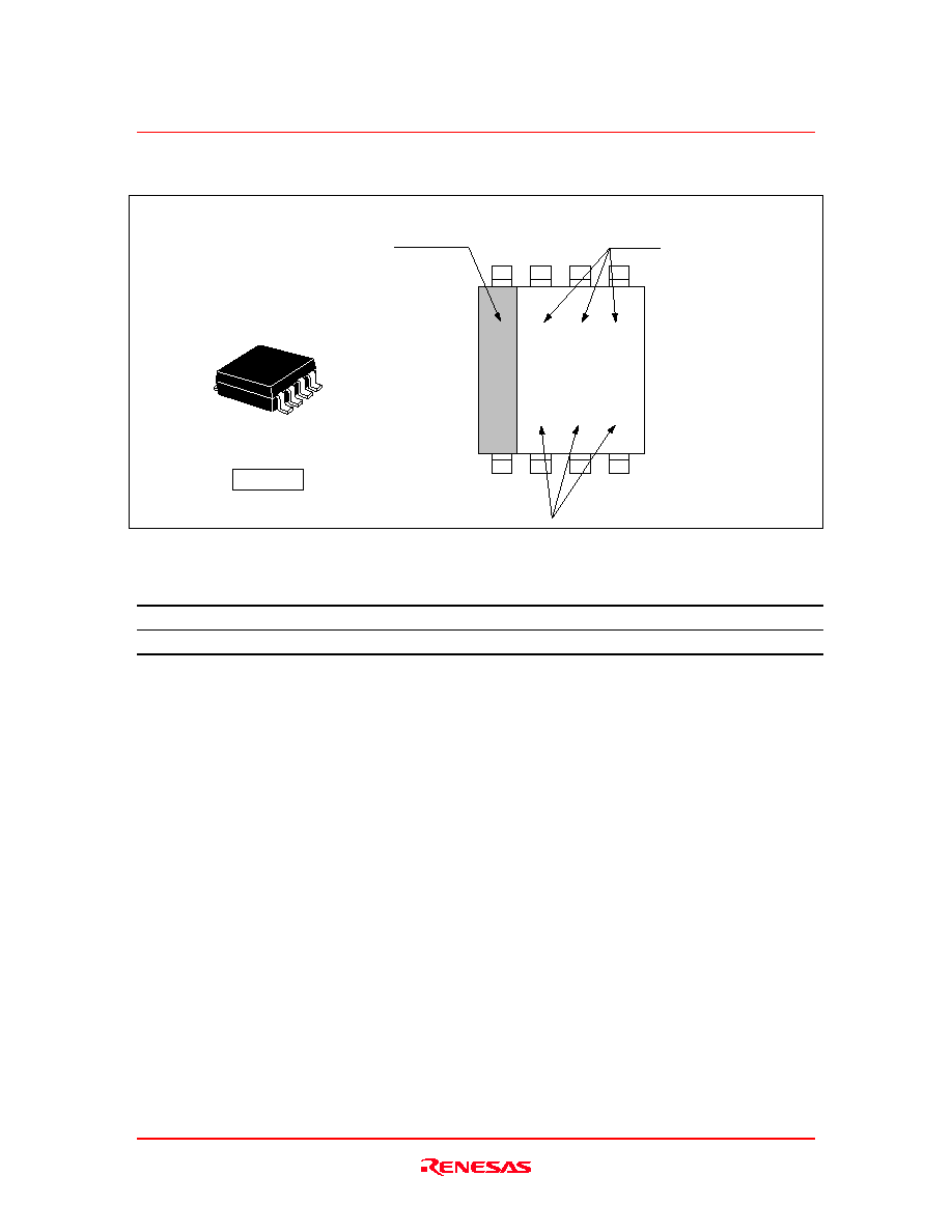
Outline and Article Indication
∑ HD74LV2G66A
Lot No.
Y : Year code
(the last digit of year)
M : Month code
W : Week code
Y M W
L 6 6
Marking
Index band
SSOP≠8
Function Table
Control
Switch
L
OFF
H
ON
H : High level
L : Low level

HD74LV2G66A
Rev.4.00, Sep.30.2003, page 3 of 11
Pin Arrangement
(Top view)
8
V
CC
1
7
CONT1
6
OUT / IN2
5
IN / OUT2
IN / OUT1
2
OUT / IN1
3
CONT2
4
GND
Absolute Maximum Ratings
Item
Symbol
Ratings
Unit
Test Conditions
Supply voltage range
V
CC
≠0.5 to 7.0
V
Input voltage range
*1
V
I
≠0.5 to 7.0
V
Output voltage range
*1, 2
V
O
≠0.5 to V
CC
+ 0.5
V
Output : H or L
Input clamp current
I
IK
≠20
mA
V
I
< 0
Output clamp current
I
OK
±50
mA
V
O
< 0 or V
O
> V
CC
Continuous output current
I
O
±25
mA
V
O
= 0 to V
CC
Continuous current through
V
CC
or GND
I
CC
or I
GND
±50
mA
Maximum power dissipation
at Ta = 25∞C (in still air)
*3
P
T
200
mW
Storage temperature
Tstg
≠65 to 150
∞C
Notes:
The absolute maximum ratings are values, which must not individually be exceeded, and
furthermore no two of which may be realized at the same time.
1. The input and output voltage ratings may be exceeded if the input and output clamp-current
ratings are observed.
2. This value is limited to 5.5 V maximum.
3. The maximum package power dissipation was calculated using a junction temperature of 150∞C.

HD74LV2G66A
Rev.4.00, Sep.30.2003, page 4 of 11
Recommended Operating Conditions
Item
Symbol
Min
Max
Unit
Conditions
Supply voltage range
V
CC
1.65
5.5
V
Input voltage range
V
I
0
5.5
V
Input / output voltage range
V
I/O
0
V
CC
V
0
300
V
CC
= 1.65 to 1.95 V
0
200
V
CC
= 2.3 to 2.7 V
0
100
V
CC
= 3.0 to 3.6 V
Input transition rise or fall rate
t /
v
0
20
ns / V
V
CC
= 4.5 to 5.5 V
Operating free-air temperature T
a
≠40
85
∞C
Note: Unused or floating control inputs must be held high or low.
HD74LV2G66A
Rev.4.00, Sep.30.2003, page 5 of 11
Electrical Characteristic
Ta = 25∞C
Ta = ≠40 to 85∞C
Item
Symbol VCC (V)
Min Typ Max Min
Typ Max
Unit Test
Conditions
1.65 to 1.95
--
--
--
V
CC
◊
0.75
--
--
2.3 to 2.7
--
--
--
V
CC
◊
0.7 --
--
3.0 to 3.6
--
--
--
V
CC
◊
0.7 --
--
V
IH
4.5 to 5.5
--
--
--
V
CC
◊
0.7 --
--
1.65 to 1.95
--
--
--
--
--
V
CC
◊
0.25
2.3 to 2.7
--
--
--
--
--
V
CC
◊
0.3
3.0 to 3.6
--
--
--
--
--
V
CC
◊
0.3
Input voltage
V
IL
4.5 to 5.5
--
--
--
--
--
V
CC
◊
0.3
V
Control input
only
1.8
--
--
--
--
0.25 --
2.5
--
--
--
--
0.30 --
3.3
--
--
--
--
0.35 --
Hysteresis
voltage
V
H
5.0
--
--
--
--
0.45 --
V
V
T
+
≠ V
T
≠
1.65
--
120 360 --
--
450
2.3
--
60
180 --
--
225
3.0
--
50
150 --
--
190
On-state switch
resistance
R
ON
4.5
--
40
75
--
--
100
V
IN
= V
CC
or GND
V
C
= V
IH
I
T
= 1 mA
1.65
--
400 1100 --
--
1400
2.3
--
200 500 --
--
600
3.0
--
90
180 --
--
225
Peak on
resistance
R
ON (P)
4.5
--
50
100 --
--
125
V
IN
= V
CC
to GND
V
C
= V
IH
I
T
= 1 mA
1.65
--
40
120 --
--
160
2.3
--
20
30
--
--
40
3.0
--
10
20
--
--
30
Difference of
on- state
resistance
between
switches
R
ON
4.5
--
7
15
--
--
20
V
IN
= V
CC
to GND
V
C
= V
IH
I
T
= 1 mA
Off-state switch
leakage current
I
s (OFF)
5.5
--
--
±0.1 --
--
±1.0
µ
A
V
IN
= V
CC
,
V
OUT
= GND
or V
IN
= GND,
V
O
= V
CC
, V
C
=
V
IL
On-state switch
leakage current
I
s (ON)
5.5
--
--
±0.1 --
--
±1.0
µ
A
V
IN
= V
CC
or GND
V
C
= V
IH
Input current
I
IN
0 to 5.5
--
--
±0.1 --
--
±1.0
µ
A
V
IN
= 5.5 V or
GND
Quiescent
supply current
I
CC
5.5
--
--
--
--
--
10
µ
A
V
IN
= V
CC
or GND
Control input
capacitance
C
IC
--
--
3.5
--
--
--
--
pF
Switch terminal
capacitance
C
IN / OUT
--
--
4.0
--
--
--
--
pF
Feed through
capacitance
C
IN≠OUT
--
--
0.5
--
--
--
--
pF