Rev.2.00, Oct.23.2003, page 1 of 9
HD74LV2GT245A
Dual Bus Transceivers with 3≠state Outputs /
CMOS Logic Level Shifter
REJ03D0153≠0200Z
(Previous ADE-205-694A (Z))
Rev.2.00
Oct.23.2003
Description
The HD74LV2GT245A has two buffers with three state output in a 8 pin package. When DIR is high, data
is transferred from the A inputs to the B outputs, and when DIR is low, data is transferred from the B inputs
to the A outputs. The A and B buses are separated by making the enable input (
OE) high level. The input
protection circuitry on this device allows over voltage tolerance on the input, allowing the device to be used
as a logic≠level translator from 3.0 V CMOS Logic to 5.0 V CMOS Logic or from 1.8 V CMOS logic to
3.0 V CMOS Logic while operating at the high-voltage power supply. Low voltage and high-speed
operation is suitable for the battery powered products (e.g., notebook computers), and the low power
consumption extends the battery life.
Features
∑
The basic gate function is lined up as Renesas uni logic series.
∑
Supplied on emboss taping for high-speed automatic mounting.
∑
TTL compatible input level.
Supply voltage range : 3.0 to 5.5 V
Operating temperature range : ≠40 to +85∞C
∑
Logic-level translate function
3.0 V CMOS logic
5.0 V CMOS logic (@V
CC
= 5.0 V)
1.8 V or 2.5 V CMOS logic
3.3 V CMOS logic (@V
CC
= 3.3 V)
∑
All inputs V
IH
(Max.) = 5.5 V (@V
CC
= 0 V to 5.5 V)
All outputs V
O
(Max.) = 5.5 V (@V
CC
= 0 V, Output : Z)
∑
Output current ±6 mA (@V
CC
= 3.0 V to 3.6 V), ±12 mA (@V
CC
= 4.5 V to 5.5 V)
∑
All the logical input has hysteresis voltage for the slow transition.
∑
Ordering Information
Part Name
Package Type
Package Code
Package
Abbreviation
Taping Abbreviation
(Quantity)
HD74LV2GT245AUSE SSOP-8 pin
TTP-8DBV
US
E (3,000 pcs/reel)
HD74LV2GT245A
Rev.2.00, Oct.23.2003, page 2 of 9
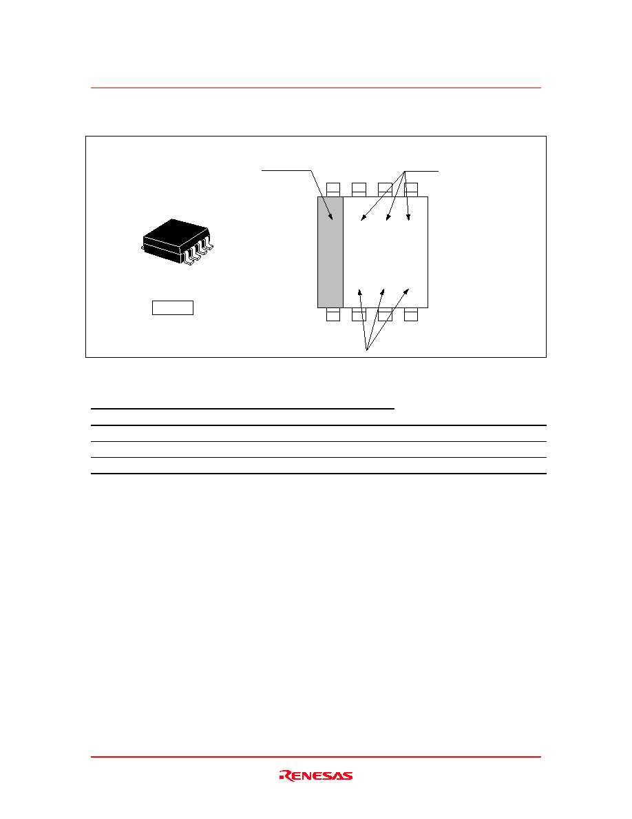
Outline and Article Indication
∑ HD74LV2GT245A
Lot No.
Y : Year code
(the last digit of year)
M : Month code
W : Week code
Y M W
T 4 5
Marking
Index band
SSOP-8
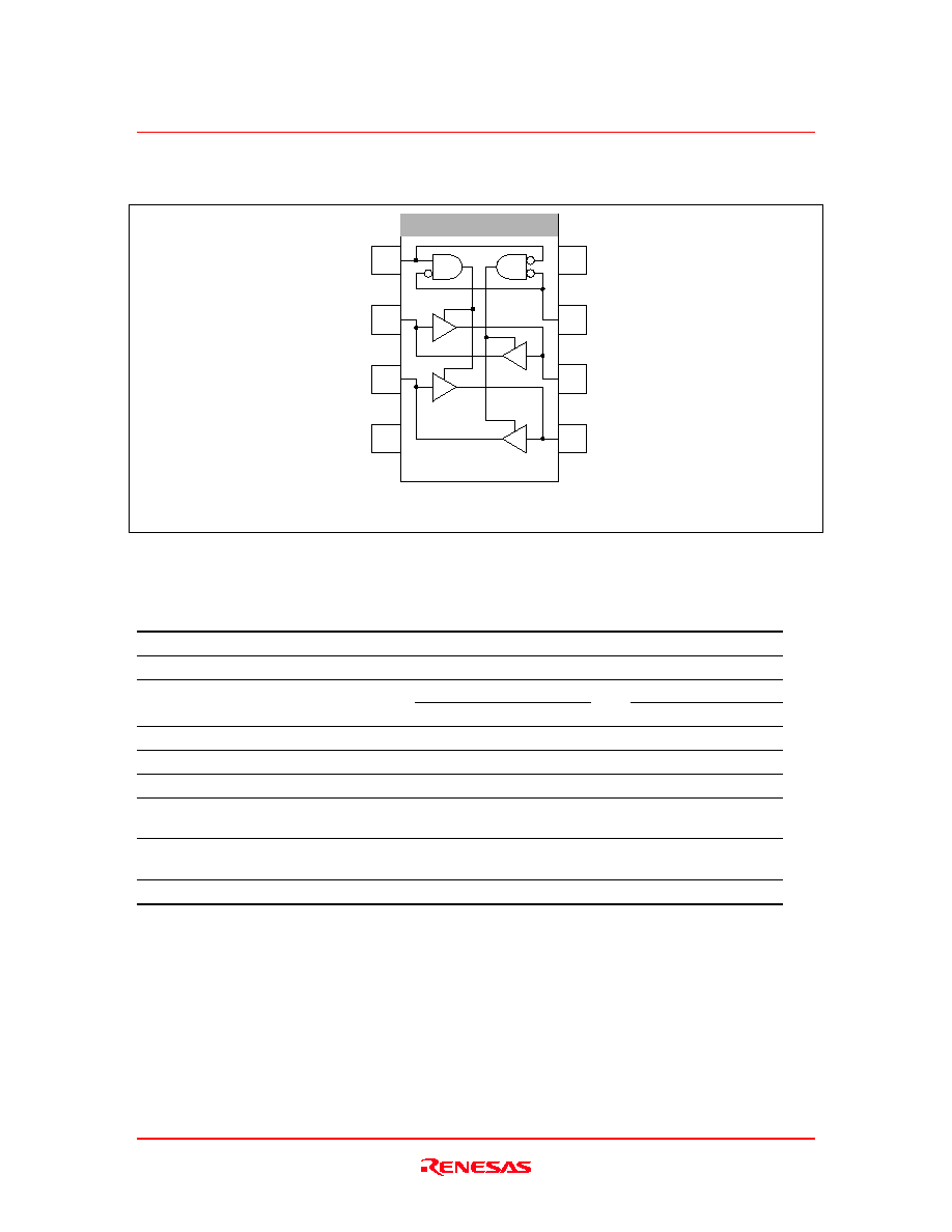
Function Table
Inputs
OE
DIR
Operation
L
L
B data to A bus
L
H
A data to B bus
H
X
Isolation
H : High level
L : Low level
X : Immaterial
HD74LV2GT245A
Rev.2.00, Oct.23.2003, page 3 of 9
Pin Arrangement
(Top view)
8
V
CC
1
7
OE
6
B1
5
B2
DIR
2
A1
3
A2
4
GND
Absolute Maximum Ratings
Item
Symbol
Ratings
Unit Test Conditions
Supply voltage range
V
CC
≠0.5 to 7.0
V
Input voltage range
*1
V
I
≠0.5 to 7.0
V
≠0.5 to V
CC
+ 0.5
Output : H or L
Output voltage range
*1, 2
V
O
≠0.5 to 7.0
V
V
CC
: OFF or output : Z
Input clamp current
I
IK
≠20
mA
V
I
< 0
Output clamp current
I
OK
±50
mA
V
O
< 0 or V
O
> V
CC
Continuous output current
I
O
±25
mA
V
O
= 0 to V
CC
Continuous current through
V
CC
or GND
I
CC
or I
GND
±50
mA
Maximum power dissipation
at Ta = 25∞C (in still air)
*3
P
T
200
mW
Storage temperature
Tstg
≠65 to 150
∞C
Notes:
The absolute maximum ratings are values, which must not individually be exceeded, and
furthermore no two of which may be realized at the same time.
1. The input and output voltage ratings may be exceeded if the input and output clamp-current
ratings are observed.
2. This value is limited to 5.5 V maximum.
3. The maximum package power dissipation was calculated using a junction temperature of 150∞C.
HD74LV2GT245A
Rev.2.00, Oct.23.2003, page 4 of 9
Recommended Operating Conditions
Item
Symbol
Ratings
Unit
Test Conditions
Supply voltage
V
CC
3.0 to 5.5
V
Input voltage
V
IN
0 to 5.5
V
0 to V
CC
Output voltage
V
OUT
0 to 5.5
V
Output : Z
Operating temperature
T
opr
≠40 to +85
∞C
0 to 100 (V
CC
= 3.0 to 3.6 V)
Input rise / fall time
t
r
, t
f
0 to 20 (V
CC
= 4.5 to 5.5 V)
ns
HD74LV2GT245A
Rev.2.00, Oct.23.2003, page 5 of 9
Electrical Characteristics
∑
Ta = ≠40 to 85∞C
Item
Symbol V
CC
(V) *
Min
Typ
Max
Unit
Test condition
3.0 to 3.6
1.5
--
--
V
IH
4.5 to 5.5
2.0
--
--
3.0 to 3.6
--
--
0.6
Input voltage
V
IL
4.5 to 5.5
--
--
0.8
V
3.3
--
0.10
--
Hysteresis voltage V
H
5.0
--
0.15
--
V
V
T
+
≠ V
T
≠
Min to Max
V
CC
≠0.1
--
--
I
OH
= ≠50
µ
A
3.0
2.48
--
--
I
OH
= ≠6 mA
V
OH
4.5
3.8
--
--
I
OH
= ≠12 mA
Min to Max
--
--
0.1
I
OL
= 50
µ
A
3.0
--
--
0.44
I
OL
= 6 mA
Output voltage
V
OL
4.5
--
--
0.55
V
I
OL
= 12 mA
Input current
I
IN
0 to 5.5
--
--
±1
µ
A
V
IN
= 5.5 V or GND
Off state output
current
I
OZ
Min to Max
--
--
±5
µ
A
V
O
= 5.5 V or GND
I
CC
5.5
--
--
10
µ
A
V
IN
= V
CC
or GND,
I
O
= 0
Quiescent
supply current
I
CC
5.5
--
--
1.5
mA
One input V
IN
= 3.4 V,
other input V
CC
or
GND
Output leakage
current
I
OFF
0
--
--
5
µ
A
V
O
= 5.5 V
Input capacitance C
IN
5.0
--
3.0
--
pF
V
IN
= V
CC
or GND
Output
capacitance
C
O
5.0
--
5.5
--
pF
V
O
= V
CC
or GND
Note: For conditions shown as Min or Max, use the appropriate values under recommended operating
conditions.