Rev.3.00 Jul. 01, 2004 page 1 of 8
HD74LVC1G32
2≠input OR Gate
REJ03D0010≠0300Z
Rev.3.00
Jul. 01.2004
Description
The HD74LVC1G32 has two≠input OR gate in a 5-pin package. Low voltage and high-speed operation is suitable for
the battery powered products (e.g., notebook computers), and the low power consumption extends the battery life.
Features
∑
The basic gate function is lined up as renesas uni logic series.
∑
Supply voltage range: 1.65 to 5.5 V
Operating temperature range: ≠40 to +85∞C
∑
All inputs:
V
IH
(Max.) = 5.5 V (@V
CC
= 0 V to 5.5 V)
All outputs: V
O
(Max.) = 5.5 V (@V
CC
= 0 V)
∑
Output current:
±4 mA (@V
CC
= 1.65 V)
±8 mA (@V
CC
= 2.3 V)
±24 mA (@V
CC
= 3.0 V)
±32 mA (@V
CC
= 4.5 V)
∑
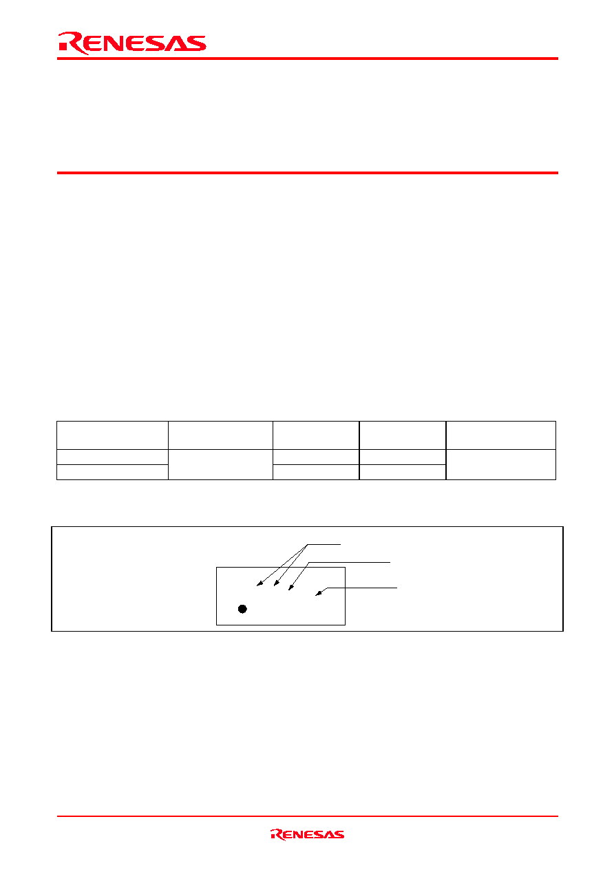
Ordering Information
Part Name
Package Type
Package Code
Package
Abbreviation
Taping Abbreviation
(Quantity)
HD74LVC1G32CPE
TBS-5V
CP
HD74LVC1G32CLE
WCSP-5 pin
TBS-5AV
CL
E (3,000 pcs/reel)
Article indication
E 4 Y M
Marking
Year code
Month code
HD74LVC1G32
Rev.3.00 Jul. 01, 2004 page 2 of 8
Function Table
Inputs
A
B
Output Y
L
L
L
H
L
H
L
H
H
H
H
H
H: High level
L: Low level
Pin Arrangement
(Bottom view)
(Top view)
OUTY
1
5
2
3
4
GND
Height 0.5 mm
0.5 mm pitch
0.17 mm 5≠Ball (CP)
0.23 mm 5≠Ball (CL)
0.9 mm
1.4 mm
INA
INB
V
CC
Pin#1 INDEX
Logic Diagram
A
B
Y

HD74LVC1G32
Rev.3.00 Jul. 01, 2004 page 3 of 8
Absolute Maximum Ratings
Item
Symbol
Ratings
Unit
Test Conditions
Supply voltage range
V
CC
≠0.5 to 6.5
V
Input voltage range
*1
V
I
≠0.5 to 6.5
V
≠0.5 to V
CC
+0.5
Output : H or L
Output voltage range
*1, 2
V
O
≠0.5 to 6.5
V
V
CC
: OFF
Input clamp current
I
IK
≠50
mA
V
I
< 0
Output clamp current
I
OK
≠50
mA
V
O
< 0
Continuous output current
I
O
±50
mA
V
O
= 0 to V
CC
Continuous current through
V
CC
or GND
I
CC
or I
GND
±100
mA
154
CP
Package Thermal impedance
ja
132
∞C/W
CL
Storage temperature
Tstg
≠65 to 150
∞C
Notes:
The absolute maximum ratings are values, which must not individually be exceeded, and furthermore no two
of which may be realized at the same time.
1. The input and output voltage ratings may be exceeded if the input and output clamp-current ratings are
observed.
2. This value is limited to 5.5 V maximum.
Recommended Operating Conditions
Item
Symbol
Min
Max
Unit
Conditions
Supply voltage range
V
CC
1.65
5.5
V
Input voltage range
V
I
0
5.5
V
Output voltage range
V
O
0
V
CC
V
--
4
V
CC
= 1.65 V
--
8
V
CC
= 2.3 V
--
16
--
24
V
CC
= 3.0 V
I
OL
--
32
V
CC
= 4.5 V
--
≠4
V
CC
= 1.65 V
--
≠8
V
CC
= 2.3 V
--
≠16
--
≠24
V
CC
= 3.0 V
Output current
I
OH
--
≠32
mA
V
CC
= 4.5 V
0
20
V
CC
= 1.65 to 1.95 V,
2.3 to 2.7 V
0
10
V
CC
= 3.0 to 3.6 V
Input transition rise or fall rate
t /
v
0
5
ns / V
V
CC
= 4.5 to 5.5 V
Operating free-air temperature
T
a
≠40
85
∞C
Note: Unused or floating inputs must be held high or low.

HD74LVC1G32
Rev.3.00 Jul. 01, 2004 page 4 of 8
Electrical Characteristics
Ta = ≠40 to 85∞C
Item
Symbol
V
CC
(V)
Min
Typ
Max
Unit
Test condition
1.65 to 1.95
V
CC
◊
0.65
--
--
2.3 to 2.7
1.7
--
--
3.0 to 3.6
2.0
--
--
V
IH
4.5 to 5.5
V
CC
◊
0.7
--
--
1.65 to 1.95
--
--
V
CC
◊
0.35
2.3 to 2.7
--
--
0.7
3.0 to 3.6
--
--
0.8
Input voltage
V
IL
4.5 to 5.5
--
--
V
CC
◊
0.3
V
Min to Max
V
CC
≠0.1
--
--
I
OH
= ≠100
µ
A
1.65
1.2
--
--
I
OH
= ≠4 mA
2.3
1.9
--
--
I
OH
= ≠8 mA
2.4
--
--
I
OH
= ≠16 mA
3.0
2.3
--
--
I
OH
= ≠24 mA
V
OH
4.5
3.8
--
--
I
OH
= ≠32 mA
Min to Max
--
--
0.1
I
OL
= 100
µ
A
1.65
--
--
0.45
I
OL
= 4 mA
2.3
--
--
0.3
I
OL
= 8 mA
--
--
0.4
I
OL
= 16 mA
3.0
--
--
0.55
I
OL
= 24 mA
Output voltage
V
OL
4.5
--
--
0.55
V
I
OL
= 32 mA
Input current
I
IN
0 to 5.5
--
--
±5
µ
A
V
IN
= 5.5 V or GND
I
CC
5.5
--
--
10
V
IN
= V
CC
or GND, I
O
= 0
Quiescent
supply current
I
CC
3 to 5.5
--
--
500
µ
A
One input at V
CC
≠0.6 V,
Other input at V
CC
or GND
Output leakage
current
I
OFF
0
--
--
±10
µ
A
V
IN
or V
O
= 0 to 5.5 V
Input capacitance
C
IN
3.3
--
4.0
--
pF
V
IN
= V
CC
or GND
Note: For conditions shown as Min or Max, use the appropriate values under recommended operating conditions.
HD74LVC1G32
Rev.3.00 Jul. 01, 2004 page 5 of 8
Switching Characteristics
V
CC
= 1.8 ± 0.15 V
Ta = ≠40 to 85∞C
Item
Symbol
Min
Max
Unit
Test Conditions
FROM
(Input)
TO
(Output)
1.9
7.2
C
L
= 15 pF, R
L
= 1 M
Propagation delay time
t
PLH
t
PHL
2.8
8.0
ns
C
L
= 30 pF, R
L
= 1.0 k
A or B
Y
V
CC
= 2.5 ± 0.2 V
Ta = ≠40 to 85∞C
Item
Symbol
Min
Max
Unit
Test Conditions
FROM
(Input)
TO
(Output)
0.8
4.4
C
L
= 15 pF, R
L
= 1 M
Propagation delay time
t
PLH
t
PHL
1.2
5.5
ns
C
L
= 30 pF, R
L
= 500
A or B
Y
V
CC
= 3.3 ± 0.3 V
Ta = ≠40 to 85∞C
Item
Symbol
Min
Max
Unit
Test Conditions
FROM
(Input)
TO
(Output)
0.9
3.6
C
L
= 15 pF, R
L
= 1 M
Propagation delay time
t
PLH
t
PHL
1.1
4.5
ns
C
L
= 50 pF, R
L
= 500
A or B
Y
V
CC
= 5.0 ± 0.5 V
Ta = ≠40 to 85∞C
Item
Symbol
Min
Max
Unit
Test Conditions
FROM
(Input)
TO
(Output)
0.8
3.4
C
L
= 15 pF, R
L
= 1 M
Propagation delay time
t
PLH
t
PHL
1.0
4.0
ns
C
L
= 50 pF, R
L
= 500
A or B
Y
Operating Characteristics
Ta = 25∞C
Item
Symbol
V
CC
(V)
Min
Typ
Max
Unit
Test Conditions
1.8
--
20
--
2.5
--
20
--
3.3
--
21
--
Power dissipation capacitance
C
PD
5.0
--
22
--
pF
f = 10 MHz
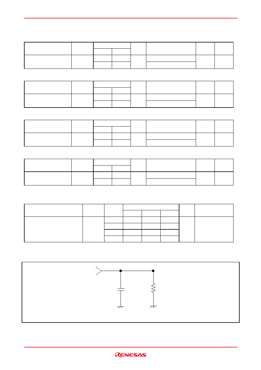
Test Circuit
L
Note: C includes probe and jig capacitance.
C
L
Measurement point
R
L
*
From Output