Rev.3.00 Jul. 01, 2004 page 1 of 10
HD74LVC1G66
Single Analog Switch
REJ03D0026≠0300Z
Rev.3.00
Jul. 01, 2004
Description
The HD74LVC1G66 has an analog switch in a 5-pin package. Switch section has its enable input control (CONT).
High-level voltage applied to CONT turns on the switch section. Applications include signal gating chopping,
modulation or demodulation (modem), and signal multiplexing for analog to digital to analog conversion systems. Low
voltage and high-speed operation is suitable for the battery powered products (e.g., notebook computers), and the low
power consumption extends the battery life.
Features
∑
The basic gate function is lined up as renesas uni logic series.
∑
Supply voltage range: 1.65 to 5.5 V
Operating temperature range: ≠40 to +85∞C
∑
Control input: V
IH
(Max.) = 5.5 V (@V
CC
= 0 V to 5.5 V)
∑
Ordering Information
Part Name
Package Type
Package Code
Package
Abbreviation
Taping Abbreviation
(Quantity)
HD74LVC1G66CPE
TBS-5V
CP
HD74LVC1G66CLE
WCSP-5 pin
TBS-5AV
CL
E (3,000 pcs/reel)
Article Indication
E 9 Y M
Marking
Year code
Month code
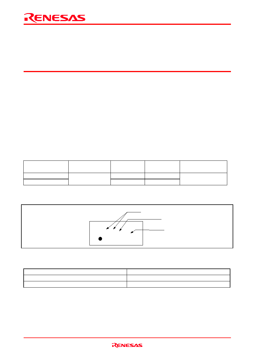
Function Table
Control
Switch
L
OFF
H
ON
H: High level
L: Low level
HD74LVC1G66
Rev.3.00 Jul. 01, 2004 page 2 of 10
Pin Arrangement
(Bottom view)
(Top view)
CONT
1
5
2
3
4
GND
Height 0.5 mm
0.5 mm pitch
0.17 mm 5≠Ball (CP)
0.23 mm 5≠Ball (CL)
0.9 mm
1.4 mm
OUT/IN
IN/OUT
V
CC
Pin#1 INDEX
Logic Diagram
IN/OUT
OUT/IN
C
O
NT
1
4
2
Absolute Maximum Ratings
Item
Symbol
Ratings
Unit
Test Conditions
Supply voltage range
V
CC
≠0.5 to 6.5
V
Input voltage range
*1
V
I
≠0.5 to 6.5
V
Output voltage range
*1, 2
V
O
≠0.5 to V
CC
+0.5
V
Output : H or L
Control Input clamp current
I
IK
≠50
mA
V
I
< 0
Output clamp current
I
OK
±50
mA
V
O
< 0 or V
O
> V
CC
Continuous output current
I
O
±50
mA
V
O
= 0 to V
CC
Continuous current through
V
CC
or GND
I
CC
or I
GND
±100
mA
154
CP
Package Thermal impedance
ja
132
∞C/W
CL
Storage temperature
Tstg
≠65 to 150
∞C
Notes:
The absolute maximum ratings are values, which must not individually be exceeded, and furthermore no two
of which may be realized at the same time.
1. The input and output voltage ratings may be exceeded if the input and output clamp-current ratings are
observed.
2. This value is limited to 5.5 V maximum.
HD74LVC1G66
Rev.3.00 Jul. 01, 2004 page 3 of 10
Recommended Operating Conditions
Item
Symbol
Min
Max
Unit
Conditions
Supply voltage range
V
CC
1.65
5.5
V
Control Input voltage range
V
I
0
5.5
V
Input/Output voltage range
V
I/O
0
V
CC
V
0
20
V
CC
= 1.65 to 1.95 V,
2.3 to 2.7 V
0
10
V
CC
= 3.0 to 3.6 V
Input transition rise or fall rate
t /
v
0
10
ns / V
V
CC
= 4.5 to 5.5 V
Operating free-air temperature
T
a
≠40
85
∞C
Note: Unused or floating inputs must be held high or low.
Electrical Characteristics
Ta = ≠40 to 85∞C
Item
Symbol
V
CC
(V)
Min
Typ
Max
Unit
Test condition
1.65 to 1.95
V
CC
◊
0.65
--
--
2.3 to 2.7
V
CC
◊
0.7
--
--
3.0 to 3.6
V
CC
◊
0.7
--
--
V
IH
4.5 to 5.5
V
CC
◊
0.7
--
--
1.65 to 1.95
--
--
V
CC
◊
0.35
2.3 to 2.7
--
--
V
CC
◊
0.3
3.0 to 3.6
--
--
V
CC
◊
0.3
Input voltage
V
IL
4.5 to 5.5
--
--
V
CC
◊
0.3
V
1.65
--
13
30
I
S
= 4 mA
2.3
--
9
20
I
S
= 8 mA
3.0
--
7.5
15
I
S
= 24 mA
On≠state switch
resistance
R
ON
4.5
--
5.5
10
I
S
= 32 mA
V
I
=V
CC
or GND
1.65
--
74.5
120
I
S
= 4 mA
2.3
--
20
30
I
S
= 8 mA
3.0
--
11.5
20
I
S
= 24 mA
Peak on resistance R
ON
(P)
4.5
--
7.5
15
I
S
= 32 mA
V
I
=V
CC
to GND
--
--
±1.0
Off-state switch
leakage current
I
S (OFF)
5.5
--
--
±0.1*
1
µ
A
V
I
= V
CC
and V
O
= GND or
V
I
= GND and V
O
= V
CC
,
V
C
= V
IL
--
--
±1.0
On-state switch
leakage current
I
S (ON)
5.5
--
--
±0.1*
1
µ
A
V
I
= V
CC
or GND, V
C
= V
IH
V
O
= Open
--
--
±1.0
Control input
current
I
IN
5.5
--
--
±0.1*
1
µ
A
V
IN
= V
CC
or GND
--
--
10
I
CC
5.5
--
--
1.0*
1
µ
A
V
IN
= V
CC
or GND
Quiescent
supply current
I
CC
5.5
--
--
500
µ
A
V
C
= V
CC
≠0.6 V
Control input
capacitance
C
IC
5.0
--
3.0
--
pF
C
I/O(OFF)
5.0
--
6.0
--
Switch terminal
capacitance
C
I/O(ON)
5.0
--
13
--
pF
Note:
1. Ta = 25∞C

HD74LVC1G66
Rev.3.00 Jul. 01, 2004 page 4 of 10
Switching Characteristics
V
CC
= 1.8 ± 0.15 V
Ta = ≠40 to 85∞C
Item
Symbol
Min
Max
Unit
Test Conditions
FROM
(Input)
TO
(Output)
Propagation delay time*
1
t
PLH
t
PHL
2.0
C
L
= 30 pF, R
L
= 1.0 k
INOUT or
OUTIN
OUTIN or
INOUT
Enable time
t
ZH
t
ZL
2.5
12.0
C
L
= 30 pF, R
L
= 1.0 k
CONT
INOUT or
OUTIN
Disable time
t
HZ
t
LZ
2.2
10.0
ns
C
L
= 30 pF, R
L
= 1.0 k
CONT
INOUT or
OUTIN
V
CC
= 2.5 ± 0.2 V
Ta = ≠40 to 85∞C
Item
Symbol
Min
Max
Unit
Test Conditions
FROM
(Input)
TO
(Output)
Propagation delay time*
1
t
PLH
t
PHL
1.2
C
L
= 30 pF, R
L
= 500
INOUT or
OUTIN
OUTIN or
INOUT
Enable time
t
ZH
t
ZL
1.9
6.5
C
L
= 30 pF, R
L
= 500
CONT
INOUT or
OUTIN
Disable time
t
HZ
t
LZ
1.4
6.9
ns
C
L
= 30 pF, R
L
= 500
CONT
INOUT or
OUTIN
V
CC
= 3.3 ± 0.3 V
Ta = ≠40 to 85∞C
Item
Symbol
Min
Max
Unit
Test Conditions
FROM
(Input)
TO
(Output)
Propagation delay time*
1
t
PLH
t
PHL
0.8
C
L
= 50 pF, R
L
= 500
INOUT or
OUTIN
OUTIN or
INOUT
Enable time
t
ZH
t
ZL
1.8
5.0
C
L
= 50 pF, R
L
= 500
CONT
INOUT or
OUTIN
Disable time
t
HZ
t
LZ
2.0
6.5
ns
C
L
= 50 pF, R
L
= 500
CONT
INOUT or
OUTIN
V
CC
= 5.0 ± 0.5 V
Ta = ≠40 to 85∞C
Item
Symbol
Min
Max
Unit
Test Conditions
FROM
(Input)
TO
(Output)
Propagation delay time*
1
t
PLH
t
PHL
0.6
C
L
= 50 pF, R
L
= 500
INOUT or
OUTIN
OUTIN or
INOUT
Enable time
t
ZH
t
ZL
1.5
4.2
C
L
= 50 pF, R
L
= 500
CONT
INOUT or
OUTIN
Disable time
t
HZ
t
LZ
1.4
5.0
ns
C
L
= 50 pF, R
L
= 500
CONT
INOUT or
OUTIN
Note:
1. The propagation delay is calculated RC time constant of typical on-state resistance of the switch and the
specified load capacitance, when driven by an ideal voltage source (zero output impedance).
HD74LVC1G66
Rev.3.00 Jul. 01, 2004 page 5 of 10
Analog Switch Characteristics
Ta = 25∞C
Item
V
CC
(V)
Min
Typ Max Unit
Test conditions
FROM
(Input)
TO
(Output)
1.65
--
35
--
2.3
--
120
--
3.0
--
175
--
4.5
--
195
--
C
L
= 50 pF,
R
L
= 600
1.65
--
>300 --
2.3
--
>300 --
3.0
--
>300 --
Frequency response
(Switch ON)
4.5
--
>300 --
MHz
C
L
= 5 pF,
R
L
= 50
Adjust fin voltage to obtain
0dBm at output when fin is
1MHz (sine wave).
Increase fin frequency until
the dB≠meter reads ≠3 dBm.
20 log(V
O
/V
I
) = ≠3 dBm
INOUT or
OUTIN
OUTIN or
INOUT
1.65
--
35
--
2.3
--
50
--
3.0
--
70
--
Crosstalk
(Control input to signal
output)
4.5
--
100
--
mV C
L
= 50 pF,
R
L
= 600
Adjust RL value to obtain 0A
at I
IN/OUT
when fin is 1MHz
(square wave)
CONT
OUTIN or
INOUT
1.65
--
≠58
--
2.3
--
≠58
--
3.0
--
≠58
--
4.5
--
≠58
--
C
L
= 50 pF,
R
L
= 600
1.65
--
≠42
--
2.3
--
≠42
--
3.0
--
≠42
--
Feed through
attenuation
(Switch OFF)
4.5
--
≠42
--
dB
C
L
= 5 pF,
R
L
= 50
Adjust fin voltage to obtain
0dBm at input when fin is
1MHz (sine≠wave)
INOUT or
OUTIN
OUTIN or
INOUT
1.65
--
0.1
--
2.3
--
0.025 --
3.0
--
0.015 --
4.5
--
0.01 --
C
L
= 50 pF,
R
L
= 10 k
fin = 1 kHz
(sine≠wave)
1.65
--
0.15 --
2.3
--
0.025 --
3.0
--
0.015 --
Sine≠wave distortion
4.5
--
0.01 --
%
C
L
= 50 pF,
R
L
= 10 k
fin = 10 kHz
(sine≠wave)
V
I
=1.4V
P≠P
, V
CC
=1.65V
V
I
=2.0V
P≠P
, V
CC
=2.3V
V
I
=2.5V
P≠P
, V
CC
=3.0V
V
I
=4.0V
P≠P
, V
CC
=4.5V
INOUT or
OUTIN
OUTIN or
INOUT
Operating Characteristics
Ta = 25∞C
Item
Symbol
V
CC
(V)
Min
Typ
Max
Unit
Test Conditions
1.8
--
8
--
2.5
--
9
--
3.3
--
9
--
Power dissipation capacitance
C
PD
5.0
--
11
--
pF
f = 10 MHz

HD74LVC1G66
Rev.3.00 Jul. 01, 2004 page 6 of 10
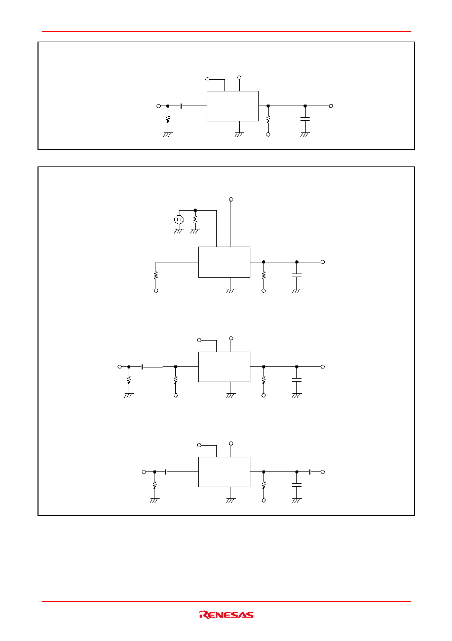
Test Circuit
V
OUT
V
CC
+
≠
V
CC
GND
(ON)
V
V =V
C
IH
V =V
∑ R
ON
IN
CC
I
S
V
IN≠OUT
R =
ON
I
S
()
V
IN≠OUT
V
CC
V
CC
GND
(OFF)
A
V =V
C
IL
V =V
or GND
IN
CC
V =GND
or V
OUT
CC
V
CC
V
CC
GND
(ON)
A
V =V
C
IH
V =V
or GND
IN
CC
V
OPEN
OUT
∑ I (off), I (on)
S
S

HD74LVC1G66
Rev.3.00 Jul. 01, 2004 page 7 of 10
Test Circuit (cont.)
OPEN
OPEN
TEST
S1
VTT
VTT
S1
C
L
R
L
R
L
GND
GND
t / t
PLH
PHL
t / t
ZH
HZ
t / t
ZL
LZ
1.8±0.15
2.5±0.2
3.3±0.3
5.0±0.5
INPUTS
V
CC
(V)
V
CC
2
◊
V
CC
2
◊
V
CC
2
◊
V
CC
2
◊
V
CC
V
CC
/ 2
V
CC
/ 2
V
CC
/ 2
V
CC
/ 2
V
CC
V
CC
V
CC
V
I
V
ref
C
L
R
L
V
VTT
t
r
/ t
f
500
0.15 V
0.15 V
0.3 V
0.3 V
500
500
1.0 k
Load circuit
From Output
2 ns
2 ns
2.5 ns
2.5 ns
30 pF
30 pF
50 pF
50 pF
V
ref
V
ref
V
ref
V
ref
V
I
0 V
t
PLH
V
t
PHL
OH
V
OL
Input
Output
V
OH
V
OL
Control
Input
V
ref
V
ref
V
ref
V
OH
≠
V
V
OL
+
V
V
ref
V
I
V
OH
0 V
V
OL
t
HZ
t
LZ
t
ZH
t
ZL
Output
(Waveform ≠ A)
Output
(Waveform ≠ B)
Notes: 1. C
L
includes probe and jig capacitance.
2. Waveform≠A is for an output with internal conditions such that the output is low except
when disabled by the output control.
3. Waveform≠B is for an output with internal conditions such that the output is high except
when disabled by the output control.
4. All input pulses are supplied by generators having the following characteristics:
PRR
10MHz, Zo = 50
.
5. The output are measured one at a time with one transition per measurement.
HD74LVC1G66
Rev.3.00 Jul. 01, 2004 page 8 of 10
Frequency response (Switch ON)
V
CC
V = V
0.1
µ
F
C
V
IN
V
OUT
IH
V
CC
f
in
f = sine wave
in
GND
(ON)
C = 50 pF
L
R = 600
L
R = 50
L
V /2
CC
or 50
or 5 pF
Feedthrough attenuation (Switch OFF)
V
CC
V = V
0.1
µ
F
C
V
IN
V
OUT
V /2
CC
IL
V
CC
f
in
GND
(OFF)
C = 50 pF or 5 pF
L
R =
600
L
V /2
CC
R =
600
L
R =
50
L
600
Crosstalk (Control input to signal output)
V
OUT
V /2
CC
C = 50 pF
L
R =
600
L
V /2
CC
R =
600
L
V
CC
V
C
V
CC
GND
R =
50
L
Sine-wave distortion
V
CC
V = V
10
µ
F
C
V
IN
V
OUT
V /2
CC
IH
V
CC
f
in
GND
10
µ
F
(ON)
C = 50 pF
L
R =
10 k
L
or 50
or 50

HD74LVC1G66
Rev.3.00 Jul. 01, 2004 page 9 of 10
Package Dimensions
TBS-5V
EIAJ Package Code
JEDEC Code
Mass (g)
Lead Material
0.001
Symbol
Dimension in Millimeters
Min
Typ
Max
A
0.50
0.15
0.35
0.05
0.05
0.20
0.19
0.90
1.40
0.50
0.20
0.20
0.15
0.17
0.10
A
1
A
2
b
D
E
e
x
y
1
y
ZD
ZE
e
e
ZD
ZE
B
C
B
A
1
2
Pin #1 index area
A
D
C
Seating plane
5
◊
b
C
x
M
A B
y C
C
x
M
A
1
A
2
A
E
y
1
C
//

HD74LVC1G66
Rev.3.00 Jul. 01, 2004 page 10 of 10
TBS-5AV
EIAJ Package Code
JEDEC Code
Mass (g)
Lead Material
0.001
Symbol
Dimension in Millimeters
Min
Nom
Max
A
0.50
0.185
(0.315)*
0.05
0.05
0.20
0.25
0.90
1.40
0.50
0.20
0.20
0.20
0.155
A
1
A
2
b
D
E
e
x
y
1
y
ZD
ZE
e
e
ZD
ZE
B
C
B
A
1
2
Pin #1 index area
A
D
C
Seating plane
*Reference value.
5
◊
b
C
x
M
A B
y C
C
x
M
A
1
A
2
A
E
y
1
C
//