 | –≠–ª–µ–∫—Ç—Ä–æ–Ω–Ω—ã–π –∫–æ–º–ø–æ–Ω–µ–Ω—Ç: HD75173P | –°–∫–∞—á–∞—Ç—å:  PDF PDF  ZIP ZIP |

Rev.2.00, Jul.16.2004, page 1 of 7
HD75173
Quadruple Differential Line Receivers With 3 State Outputs
REJ03D0310≠0200Z
(Previous ADE-205-592 (Z))
Rev.2.00
Jul.16.2004
Description
The HD75173 is a quadruple differential line receiver with three state outputs. It is designed to satisfy the requirements
of EIA standards RS-422A, RS-423A and several CCITT recommendations. Each receiver features an active high
enable and an active low enable common to all four receivers. It also features differential input sensitivity of ±200 mV.
Features
∑
Ordering Information
Part Name
Package Type
Package Code
Package
Abbreviation
Taping Abbreviation
(Quantity)
HD75173P
DILP-16 pin
DP-16E, -16FV
P
--
Function Table
Differential Inputs
Enables
Output
A-B
G
G
G
G
G
Y
V
ID
0.2 V
H
X
H
X
L
H
≠0.2 V < V
ID
< 0.2 V
H
X
?
X
L
?
V
ID
≠0.2 V
H
X
L
X
L
L
X
L
H
Z
H :
High level
L :
Low level
X :
Irrelenant
? :
Indeterminate
Z :
High impedance
HD75173
Rev.2.00, Jul.16.2004, page 2 of 7
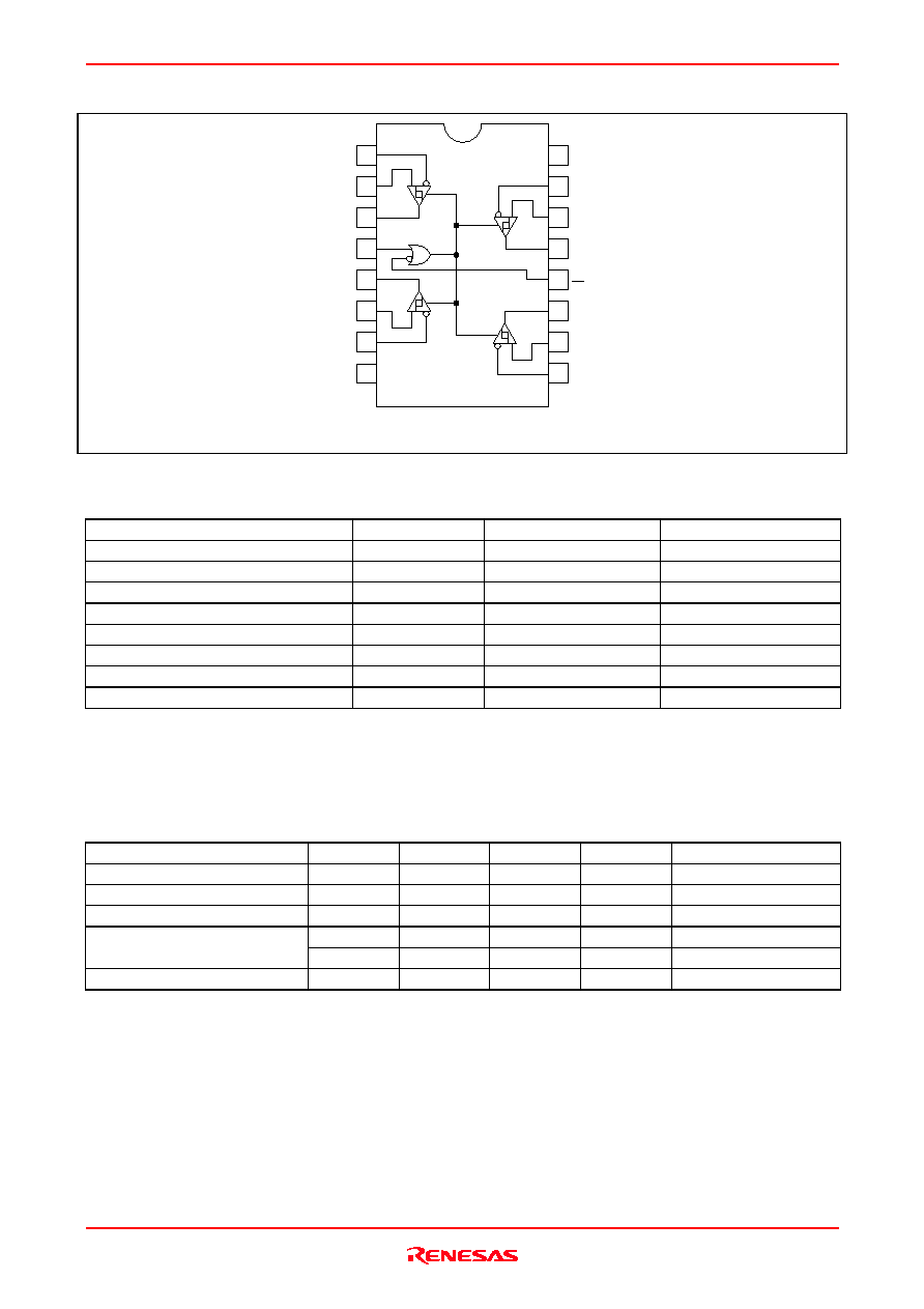
Pin Arrangement
(Top view)
1
2
3
4
5
6
7
1B
GND
1A
1Y
2Y
8
Enable
G
2A
2B
13
14
15
10
11
12
9
16 V
CC
4B
4A
4Y
Enable
G
3Y
3A
3B
Absolute Maximum Ratings
(Ta = 0 to 70∞C)
Item
Symbol
Rating
Unit
Supply Voltage
V
CC
7
V
Input Voltage, A or B Inputs
V
IN
±25
V
Differential Input Voltage*
1
V
ID
±25
V
Enable Input Voltage
V
IE
7
V
Output Current
I
OL
50
mA
Power Dissipation (Ta = 25∞C)
P
T
1150
mW
Operating temperature range
Topr
0 to 70
∞C
Storage Temperature Range
Tstg
≠65 to +150
∞C
Notes: 1. Differential input voltage is measured at the noninverting input with respect to the corresponding inverting
input
2. The absolute maximum ratings are values which must not individually be exceeded, and furthermore, no two
of which may be realized at the same time.
Recommended Operating Conditions
Item
Symbol
Min
Typ
Max
Unit
Supply Voltage
V
CC
4.75
5.00
5.25
V
Common Mode Input Voltage
V
IN
--
--
±12
V
Differential Input Voltage
V
ID
--
--
±12
V
Output Current
V
OH
--
--
≠400
µA
V
OL
--
--
16
mA
Operating Temperature
Topr
0
--
70
∞C

HD75173
Rev.2.00, Jul.16.2004, page 3 of 7
DC Electrical Characteristics
(Ta = 0 to 70∞C)
Item
Symbol
Min
Typ
*
1
Max
Unit
Conditions
Differential Input High
Threshold Voltage
V
TH
--
--
0.2
V
V
O
= 2.7 V, I
O
= ≠0.4 mA
Differential Output Low
Threshold Voltage
V
TL
≠0.2*
2
--
--
V
V
O
= 0.5 V, I
O
= 16 mA
Hysteresis
V
T
+
≠ V
T
≠
--
50
--
mV
Enable Input Voltage
V
IH
2
--
--
V
V
IL
--
--
0.8
Enable Input Clamp Voltage
V
IK
--
--
≠1.5
V
II = ≠18 mA
Output Voltage
V
OH
2.7
--
--
V
V
ID
= 200 mV, I
OH
= ≠400 µA
V
OL
--
--
0.45
V
V
ID
= ≠200 mV, I
OL
= 8 mA
--
--
0.5
V
ID
= ≠200 mV, I
OL
= 16 mA
High Impedance State
V
OZ
--
--
≠20
µA
V
O
= 0.4 V
Output Current
--
--
+20
V
O
= 2.4 V
Line Input Current
I
I
--
--
1
mA
Other Input at 0 V*
4
V
I
= 12 V
--
--
≠0.8
V
I
= ≠7 V
Enable Input Current
I
IH
--
--
20
µA
V
IH
= 2.7 V
I
IL
--
--
≠100
µA
V
IL
= 0.4 V
Input Resistance
ri
12
--
--
k
Short Circuit Output Current*
3
I
OS
≠15
--
≠85
mA
Supply Current
I
CC
--
--
70
mA
Notes: 1. All Typical Values are at V
CC
= 5 V, Ta = 25∞C
2. The algebraic convention is used in this data sheet for threshold voltage levels only.
3. Not more than one output should be shorted at a time.
4. Refer to EIA standards RS-422A and RS-423A for exact conditions.
Switching Characteristics
(V
CC
= 5 V, Ta = 25∞C)
Item
Symbol
Min
Typ
Max
Unit
Test Conditions
Propagation Delay Time
t
PLH
--
20
35
ns
C
L
= 15 pF
t
PHL
--
22
35
Output Enable Time
t
ZH
--
17
22
C
L
= 15 pF
t
ZL
--
20
25
Output Disable Time
t
HZ
--
21
30
C
L
= 5 pF
t
LZ
--
30
40
HD75173
Rev.2.00, Jul.16.2004, page 4 of 7
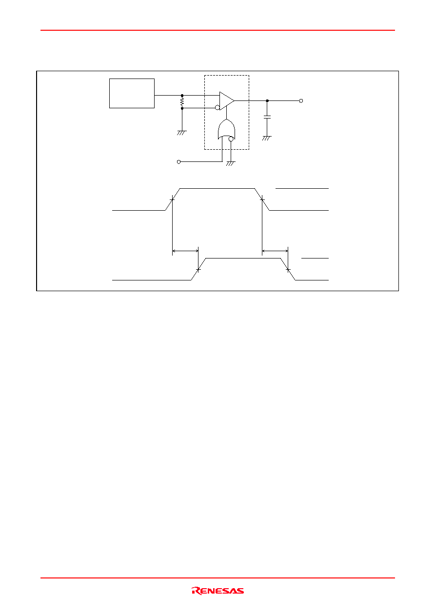
Switching Time Test Method
1. t
PLH
, t
PHL
C
15 pF
L
Output
2 V
50
Pulse
Generator
See Note 1
t
PLH
OH
V
OL
V
1.3 V
Input
0 V
0 V
2.5 V
≠2.5 V
t
PHL
1.3 V
Output
HD75173
Rev.2.00, Jul.16.2004, page 5 of 7
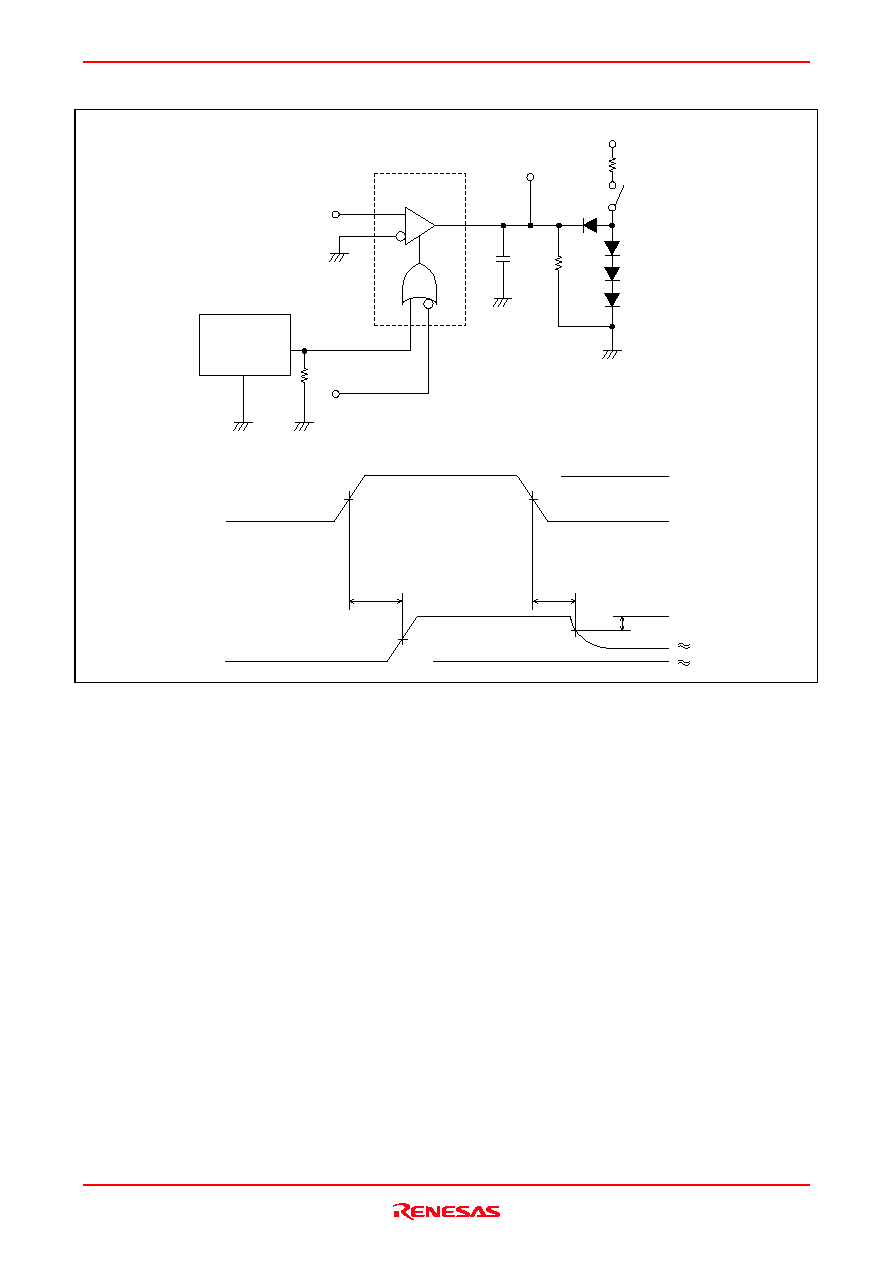
2. t
ZH
, t
ZL
2.5 V
2 V
C
L
Output
2 k
V
CC
5 k
S1
50
Pulse
Generator
See Note 1
See Note 2
See Note 3
t
ZH
OH
V
1.3 V
Input
1.3 V
1.3 V
3 V
0 V
t
HZ
0.5 V
Output
S1 : Open
1.4 V
S1 : Closed
0 V