Document Outline
- Description
- Features
- Ordering Information
- Pin Arrangement
- Pin Description
- Block Diagram
- Memory Map and Address
- Pin Function
- Mode Selection
- Command Definition
- Mode Description
- Command/Address/Data Input Sequence
- Status Transition
- Absolute Maximum Ratings
- Capacitance
- DC Characteristics
- AC Characteristics
- Timing Waveforms
- Power on and off Sequence
- Serial Read (1) (2) Timing Waveform
- Serial Read (1) with CA before SC Timing Waveform
- Serial Read (1) with CA after SC Timing Waveform
- Erase and Status Data Polling Timing Waveform (Sector Erase)
- Program (1) and Status Data Polling Timing Waveform
- Program (1) with CA before SC and Status Data Polling Timing Waveform
- Program (1) with CA after SC and Status Data Polling Timing Waveform
- Program (2) and Status Data Polling Timing Waveform
- Program (3) and Status Data Polling Timing Waveform
- Program (4) and Status Data Polling Timing Waveform
- Program (4) with CA before SC and Status Data Polling Timing Waveform
- Program (4) with CA after SC and Status Data Polling Timing Waveform
- ID and Status Register Read Timing Waveform
- Data Recovery Read Timing Waveform
- Data Recovery Write Timing Waveform
- Clear Status Register Timing Waveform
- Function Description
- Requirement for System
- Package Dimensions

Regarding the change of names mentioned in the document, such as Hitachi
Electric and Hitachi XX, to Renesas Technology Corp.
The semiconductor operations of Mitsubishi Electric and Hitachi were transferred to Renesas
Technology Corporation on April 1st 2003. These operations include microcomputer, logic, analog
and discrete devices, and memory chips other than DRAMs (flash memory, SRAMs etc.)
Accordingly, although Hitachi, Hitachi, Ltd., Hitachi Semiconductors, and other Hitachi brand
names are mentioned in the document, these names have in fact all been changed to Renesas
Technology Corp. Thank you for your understanding. Except for our corporate trademark, logo and
corporate statement, no changes whatsoever have been made to the contents of the document, and
these changes do not constitute any alteration to the contents of the document itself.
Renesas Technology Home Page: http://www.renesas.com
Renesas Technology Corp.
Customer Support Dept.
April 1, 2003
To all our customers

Cautions
Keep safety first in your circuit designs!
1. Renesas Technology Corporation puts the maximum effort into making semiconductor products better
and more reliable, but there is always the possibility that trouble may occur with them. Trouble with
semiconductors may lead to personal injury, fire or property damage.
Remember to give due consideration to safety when making your circuit designs, with appropriate
measures such as (i) placement of substitutive, auxiliary circuits, (ii) use of nonflammable material or
(iii) prevention against any malfunction or mishap.
Notes regarding these materials
1. These materials are intended as a reference to assist our customers in the selection of the Renesas
Technology Corporation product best suited to the customer's application; they do not convey any
license under any intellectual property rights, or any other rights, belonging to Renesas Technology
Corporation or a third party.
2. Renesas Technology Corporation assumes no responsibility for any damage, or infringement of any
third-party's rights, originating in the use of any product data, diagrams, charts, programs, algorithms, or
circuit application examples contained in these materials.
3. All information contained in these materials, including product data, diagrams, charts, programs and
algorithms represents information on products at the time of publication of these materials, and are
subject to change by Renesas Technology Corporation without notice due to product improvements or
other reasons. It is therefore recommended that customers contact Renesas Technology Corporation
or an authorized Renesas Technology Corporation product distributor for the latest product information
before purchasing a product listed herein.
The information described here may contain technical inaccuracies or typographical errors.
Renesas Technology Corporation assumes no responsibility for any damage, liability, or other loss
rising from these inaccuracies or errors.
Please also pay attention to information published by Renesas Technology Corporation by various
means, including the Renesas Technology Corporation Semiconductor home page
(http://www.renesas.com).
4. When using any or all of the information contained in these materials, including product data, diagrams,
charts, programs, and algorithms, please be sure to evaluate all information as a total system before
making a final decision on the applicability of the information and products. Renesas Technology
Corporation assumes no responsibility for any damage, liability or other loss resulting from the
information contained herein.
5. Renesas Technology Corporation semiconductors are not designed or manufactured for use in a device
or system that is used under circumstances in which human life is potentially at stake. Please contact
Renesas Technology Corporation or an authorized Renesas Technology Corporation product distributor
when considering the use of a product contained herein for any specific purposes, such as apparatus or
systems for transportation, vehicular, medical, aerospace, nuclear, or undersea repeater use.
6. The prior written approval of Renesas Technology Corporation is necessary to reprint or reproduce in
whole or in part these materials.
7. If these products or technologies are subject to the Japanese export control restrictions, they must be
exported under a license from the Japanese government and cannot be imported into a country other
than the approved destination.
Any diversion or reexport contrary to the export control laws and regulations of Japan and/or the
country of destination is prohibited.
8. Please contact Renesas Technology Corporation for further details on these materials or the products
contained therein.
HN29V102414 Series
1G AND type Flash Memory
More than 32,113-sector (542,581,248-bit)
◊
2
ADE-203-1265B (Z)
Rev. 1.0
Jan. 25, 2002
Description
The Hitachi HN29V102414 Series is a CMOS Flash Memory with AND type multi-level memory cells. It
has fully automatic programming and erase capabilities with a single 3.0 V power supply. The functions are
controlled by simple external commands. To fit the I/O card applications, the unit of programming and erase
is as small as (2048 + 64) bytes. Initial available sectors of HN29V102414 are more than 64,226 (98% of all
sector address) and less than 65,536 sectors.
Features
∑
On-board single power supply (V
CC
): V
CC
= 2.7 V to 3.6 V
∑
Organization
AND Flash Memory: (2048 + 64) bytes
◊
(More than 32,113 sectors)
◊ 2
Data register: (2048 + 64) bytes
◊ 2
∑
Multi-level memory cell
2 bit/per memory cell
∑
Automatic programming
Sector program time: 1.0 ms (typ)
System bus free
Address, data latch function
Internal automatic program verify function
Status data polling function
∑
Automatic erase
Single sector erase time: 1.0 ms (typ)
System bus free
Internal automatic erase verify function
Status data polling function

HN29V102414 Series
2
∑
Erase mode
Single sector erase ((2048 + 64) byte unit)
∑
Fast serial read access time:
First access time: 50
µ
s (max)
Serial access time: 50 ns (max)
∑
Low power dissipation:
I
CC1
= 2 mA (typ) (Read) (1-chip operation)
I
CC1
= 4 mA (typ) (Read) (2-chip operation)
I
CC2
= 20 mA (max) (Read) (1-chip operation)
I
CC2
= 40 mA (max) (Read) (2-chip operation)
I
SB2
= 50
µ
A (max) (Standby) (1-chip operation)
I
SB2
= 100
µ
A (max) (Standby) (2-chip operation)
I
CC3
/I
CC4
= 40 mA (max) (Erase/Program) (1-chip operation)
I
CC3
/I
CC4
= 80 mA (max) (Erase/Program) (2-chip operation)
I
SB3
= 20
µ
A (max) (Deep standby) (1-chip operation)
I
SB3
= 40
µ
A (max) (Deep standby) (2-chip operation)
∑
The following architecture is required for data reliability.
Error correction: more than 3-bit error correction per each sector read
Spare sectors: 1.8% (579 sectors)/chip (min) within usable sectors
Ordering Information
Type No.
Available sector
Package
HN29V102414T-50
More than 64,226 sectors
12.0
◊
18.40 mm
2
0.5 mm pitch
48-pin plastic TSOP I (TFP-48DA)
HN29V102414 Series
3
Pin Arrangement
1
2
3
4
5
6
7
8
9
10
11
12
13
14
15
16
17
18
19
20
21
22
23
24
48
47
46
45
44
43
42
41
40
39
38
37
36
35
34
33
32
31
30
29
28
27
26
25
V
CC
*
2
NC*
1, 2
NC*
1, 2
NC*
1, 2
V
SS
*
2
RES
*
2
RDY/
Busy
*
2
SC*
2
OE
*
2
I/O0*
2
I/O1*
2
I/O2*
2
I/O3*
2
V
CC
*
2
V
SS
*
2
I/O4*
2
I/O5*
2
I/O6*
2
I/O7*
2
CDE
*
2
WE
*
2
CE
*
2
NC*
1, 2
V
SS
*
2
V
CC
*
3
NC*
1, 3
NC*
1, 3
NC*
1, 3
V
SS
*
3
RES
*
3
RDY/
Busy
*
3
SC*
3
OE
*
3
I/O0*
3
I/O1*
3
I/O2*
3
I/O3*
3
V
CC
*
3
V
SS
*
3
I/O4*
3
I/O5*
3
I/O6*
3
I/O7*
3
CDE
*
3
WE
*
3
CE
*
3
NC*
1, 3
V
SS
*
3
(Top view)
48-pin TSOP
Note: 1. This pin can be used as the V
SS
pin.
2. Upper chip.
3. Lower chip.
HN29V102414 Series
4
Pin Description
Pin name
Function
I/O0 to I/O7
Input/output
CE
Chip enable
OE
Output enable
WE
Write enable
CDE
Command data enable
V
CC
*
1
Power supply
V
SS
*
1
Ground
RDY/
Busy
Ready/
Busy
RES
Reset
SC
Serial clock
NC
No connection
Note:
1. All V
CC
and V
SS
pins should be connected to a common power supply and a ground, respectively.

HN29V102414 Series
5
Block Diagram
32768
◊
(2048 + 64)
◊
8
memory matrix
X-decoder
Upper chip
Data register (2048 + 64)
Input
data
control
Sector
address
buffer
Y-address
counter
2048 + 64
32113 - 32768
V
SS
RES
Y-gating
Y-decoder
Read/Program/Erase control
Data
input
buffer
CE
OE
WE
SC
I/O0
to
I/O7
RDY/
Busy
V
CC
CDE
Multiplexer
Control
signal
buffer
Data
output
buffer
∑ ∑
∑ ∑ ∑
∑ ∑
∑
∑
∑
∑
∑
∑
∑
∑
∑
∑
32768
◊
(2048 + 64)
◊
8
memory matrix
X-decoder
Lower chip
Data register (2048 + 64)
Input
data
control
Sector
address
buffer
Y-address
counter
2048 + 64
32113 - 32768
V
SS
RES
Y-gating
Y-decoder
Read/Program/Erase control
Data
input
buffer
CE
OE
WE
SC
I/O0
to
I/O7
RDY/
Busy
V
CC
CDE
Multiplexer
Control
signal
buffer
Data
output
buffer
∑ ∑
∑ ∑ ∑
∑ ∑
∑
∑
∑
∑
∑
∑
∑
∑
∑
∑
HN29V102414 Series
6
Memory Map and Address
7FFFH
7FFEH
7FFDH
0002H
0001H
0000H
000H
2048 bytes
2048 bytes
2048 bytes
2048 bytes
2048 bytes
2048 bytes
64 bytes
64 bytes
64 bytes
64 bytes
64 bytes
64 bytes
32113 - 32768 sectors *
1
800H
83FH
Control bytes
2048 + 64 bytes
Column address
Sector address
Address
Sector address
Column address
Cycles
SA (1): First cycle
SA (2): Second cycle
CA (1): First cycle
CA (2): Second cycle
I/O0
A0
A8
A0
A8
I/O1
A1
A9
A1
A9
I/O2
A2
A10
A2
A10
I/O3
A3
A11
A3
A11
I/O4
A4
A12
A4
◊
I/O5
A5
A13
A5
◊
I/O6
A6
A14
A6
◊
I/O7
A7
◊
*
2
A7
◊
Notes: 1. Some failed sectors may exist in the device. The failed sectors can be recognized
by reading the sector valid data written in a part of the column address 800 to 83F
(The specific address is TBD.). The sector valid data must be read and kept outside
of the sector before the sector erase. When the sector is programmed, the sector
valid data should be written back to the sector.
2. An
◊
means "Don't care". The pin level can be set to either V
IL
or V
IH
, referred
to DC characteristics.
HN29V102414 Series
7
Pin Function
CE: CE is used to select the device. The status returns to the standby at the rising edge of CE in the reading
operation. However, the status does not return to the standby at the rising edge of
CE in the busy state in
programming and erase operation.
OE: Memory data and status register data can be read, when OE is V
IL
.
WE: Commands and address are latched at the rising edge of WE.
SC: Programming and reading data is latched at the rising edge of SC.
RES: RES pin must be kept at the V
ILR
(V
SS
±
0.2 V) level when V
CC
is turned on and off. In this way, data
in the memory is protected against unintentional erase and programming.
RES must be kept at the V
IHR
(V
CC
±
0.2 V) level during any operations such as programming, erase and read.
CDE: Commands and data are latched when CDE is V
IL
and address is latched when
CDE is V
IH
.
RDY/
Busy: The RDY/Busy indicates the program/erase status of the flash memory. The RDY/Busy signal
is initially at a high impedance state. It turns to a V
O L
level after the (40H) command in programming
operation or the (B0H) command in erase operation. After the erase or programming operation finishes, the
RDY/
Busy signal turns back to the high impedance state.
I/O0 to I/O7: The I/O pins are used to input data, address and command, and are used to output memory data
and status register data.
Mode Selection
Mode
CE
OE
WE
SC
RES CDE
RDY/
Busy
*
3
I/O0 to I/O7
Deep standby
◊
*
4
◊
◊
◊
V
ILR
◊
V
OH
High-Z
Standby
V
IH
◊
◊
◊
V
IHR
◊
V
OH
High-Z
Output disable
V
IL
V
IH
V
IH
◊
V
IHR
◊
V
OH
High-Z
Status register read*
1
V
IL
V
IL
V
IH
◊
V
IHR
◊
V
OH
Status register outputs
Command write*
2
V
IL
V
IH
V
IL
V
IL
V
IHR
V
IL
V
OH
Din
Notes: 1. Default mode after the power on is the status register read mode (refer to status transition). From
I/O0 to I/O7 pins output the status, when
CE
= V
IL
and
OE
= V
IL
(conventional read operation
condition).
2. Refer to the command definition. Data can be read, programmed and erased after commands are
written in this mode.
3. The RDY/
Busy
bus should be pulled up to V
CC
to maintain the V
OH
level while the RDY/
Busy
pin
outputs a high impedance.
4. An
◊
means "Don't care". The pin level can be set to either V
IL
or V
IH
referred to DC characteristics.
HN29V102414 Series
8
Command Definition*
1, 2
First bus cycle
Second bus cycle
Command
Bus
cycles
Operation
mode*
3
Data in
Operation
mode
Data in
Data out
Read
Serial read (1) (Without CA)
3
Write
00H
Write
SA (1)*
4
(With CA)
3 + 2h*
6
Write
00H
Write
SA (1)*
4
Serial read (2)
3
Write
F0H
Write
SA (1)*
4
Read identifier codes
1
Write
90H
Read
ID*
8, 9
Data recovery read
1
Write
01H
Read
Recovery
data
Auto erase
Single sector
4
Write
20H
Write
SA (1)*
4
Auto program Program (1)
(Without
CA*
7
)
4
Write
10H
Write
SA (1)*
4
(With CA*
7
)
4 + 2h*
6
Write
10H
Write
SA (1)*
4
Program (2)*
10
4
Write
1FH
Write
SA (1)*
4
Program (3) (Control bytes)*
7
4
Write
0FH
Write
SA (1)*
4
Program (4)
(WithoutCA*
7
) 4
Write
11H
Write
SA (1)*
4
(With CA*
7
)
4 + 2h*
6
Write
11H
Write
SA (1)*
4
Reset
1
Write
FFH
Clear status register
1
Write
50H
Data recovery write
4
Write
12H
Write
SA (1)*
4
HN29V102414 Series
9
Third bus cycle
Fourth bus cycle
Command
Bus
cycles
Operation
mode
Data in
Operation
mode
Data in
Read
Serial read (1) (Without CA)
3
Write
SA (2)*
4
(With CA)
3 + 2h*
6
Write
SA (2)*
4
Write
CA (1)*
5
Serial read (2)
3
Write
SA (2)*
4
Read identifier codes
1
Data recovery read
1
Auto erase
Single sector
4
Write
SA (2)*
4
Write
B0H*
11
Auto program Program (1)
(Without
CA*
7
)
4
Write
SA (2)*
4
Write
40H
*11, 12
(With CA*
7
)
4 + 2h*
6
Write
SA (2)*
4
Write
CA (1)
Program (2)*
10
4
Write
SA (2)*
4
Write
40H
*11, 12
Program (3) (Control bytes)*
7
4
Write
SA (2)*
4
Write
40H
*11, 12
Program (4)
(WithoutCA*
7
) 4
Write
SA (2)*
4
Write
40H
*11, 12
(With CA*
7
)
4 + 2h*
6
Write
SA (2)*
4
Write
CA (1)
Reset
1
Clear status register
1
Data recovery write
4
Write
SA (2)*
4
Write
40H
*11, 12

HN29V102414 Series
10
Fifth bus cycle
Sixth bus cycle
Command
Bus
cycles
Operation
mode
Data in
Operation
mode
Data in
Read
Serial read (1) (Without CA)
3
(With CA)
3 + 2h*
6
Write
CA (2)*
5
Serial read (2)
3
Read identifier codes
1
Data recovery read
1
Auto erase
Single sector
4
Auto program Program (1)
(Without
CA*
7
)
4
(With CA*
7
)
4 + 2h*
6
Write
CA (2)*
5
Write
40H
*11, 12
Program (2)*
10
4
Program (3) (Control bytes)*
7
4
Program (4)
(WithoutCA*
7
) 4
(With CA*
7
)
4 + 2h*
6
Write
CA (2)
Write
40H
*11, 12
Reset
1
Clear status register
1
Data recovery write
4
Notes: 1. Commands and sector address are latched at rising edge of
WE
pulses. Program data is latched
at rising edge of SC pulses.
2. The chip is in the read status register mode when
RES
is set to V
IHR
first time after the power up.
3. Refer to the command read and write mode in mode selection.
4. SA (1) = Sector address (A0 to A7), SA (2) = Sector address (A8 to A14).
5. CA (1) = Column address (A0 to A7), CA (2) = Column address (A8 to A11).
(0
A11 to A0
83FH)
6. The variable h is the input number of times of set of CA (1) and CA (2) (1
h
2048 + 64).
Set of CA (1) and CA (2) can be input without limitation.
7. By using program (1) and (3), data can additionally be programmed maximum 15 times for each
sector before erase.
8. ID = Identifier code; Manufacturer code (07H), Device code (9DH).
9. The manufacturer identifier code is output when
CDE
is low and the device identifier code is output
when
CDE
is high.
10. Before program (2) operations, data in the programmed sector must be erased.
11. No commands can be written during auto program and erase (when the RDY/
Busy
pin outputs a
V
OL
).
12. The fourth or sixth cycle of the auto program comes after the program data input is complete.

HN29V102414 Series
11
Mode Description
Read
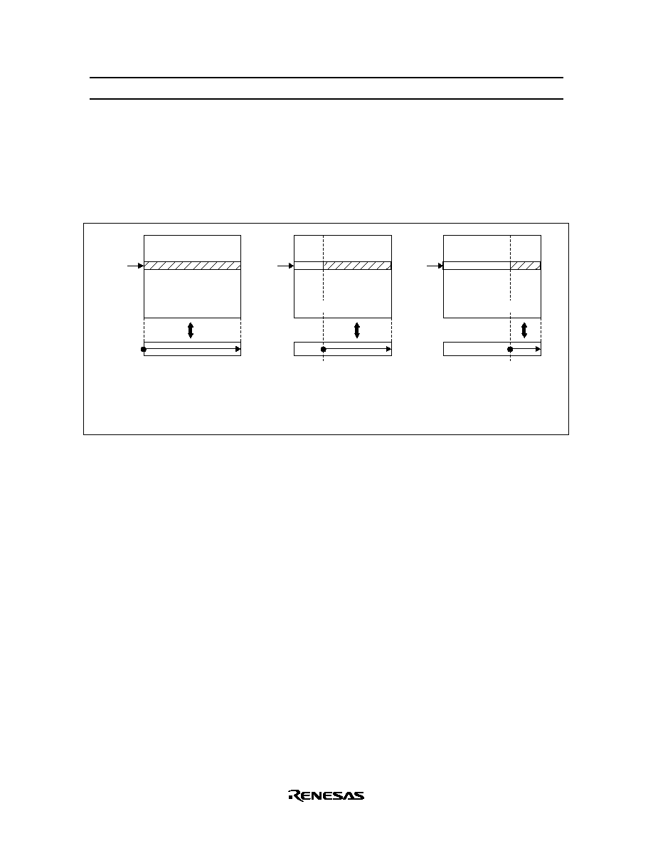
Serial Read (1): Memory data D0 to D2111 in the sector of address SA is sequentially read. Output data is
not valid after the number of the SC pulse exceeds 2112. When CA is input, memory data D (m) to D (m + j)
in the sector of address SA is sequentially read. Then output data is not valid after the number of the SC pulse
exceeds (2112 to m). The mode turns back to the standby mode at any time when
CE is V
IH
.
Serial Read (2): Memory data D2048 to D2111 in the sector of address SA is sequentially read. Output data
is not valid after the number of the SC pulse exceeds 64. The mode turns back to the standby mode at any
time when
CE is V
IH
.
Automatic Erase
Single Sector Erase: Memory data D0 to D2111 in the sector of address SA is erased automatically by
internal control circuits. After the sector erase starts, the erasure completion can be checked through the
RDY/
Busy signal and status data polling. All the bits in the sector are "1" after the erase. The sector valid
data stored in a part of memory data D2048 to D2111 must be read and kept outside of the sector before the
sector erase.
Automatic Program
Program (1): Program data PD0 to PD2111 is programmed into the sector of address SA automatically by
internal control circuits. When CA is input, program data PD (m) to PD (m + j) is programmed from CA into
the sector of address SA automatically by internal control circuits. By using program (1), data can
additionally be programed 15 times for each sector before the following erase. When the column is
programmed, the data of the column must be [FF]. After the programming starts, the program completion can
be checked through the RDY/
Busy signal and status data polling. Programmed bits in the sector turn from
"1" to "0" when they are programmed. The sector valid data should be included in the program data PD2048
to PD2111.
Program (2): Program data PD0 to PD2111 is programmed into the sector of address SA automatically by
internal control circuits. After the programming starts, the program completion can be checked through the
RDY/
Busy signal and status data polling. Programmed bits in the sector turn from "1" to "0" when they are
programmed. The sector must be erased before programming. The sector valid data should be included in the
program data PD2048 to PD2111.
Program (3): Program data PD2048 to PD2111 is programmed into the sector of address SA automatically
by internal control circuits. By using program (3), data can additionally be programed 15 times for each
sector befor the following erase. When the column is programmed, the data of the column must be [FF].
After the programming starts, the program completion can be checked through the RDY/
Busy signal and
status data polling. Programmed bits in the sector turn from "1" to "0" when they are programmed.
HN29V102414 Series
12
Program (4): Program data PD0 to PD2111 is programmed into the sector of address SA automatically by
internal control circuits. When CA is input, program data PD (m) to PD (m + j) is programmed from CA into
the sector of address SA automatically by internal control circuits. By using program (4), data can be
rewritten for each sector before the following erase. So the column data before programming operation are
either "1" or "0". In this mode, E/W number of times must be counted whenever program (4) execute. After
the programming starts, the program completion can be checked through the RDY/
Busy signal and status data
polling. The sector valid data should be included in the program data PD2048 to PD2111.
Memory array
32767
Sector
address
0
0
2111
Register
Serial read (1) (Without CA)
Program (1) (Without CA)
Program (2)
32767
Sector
address
0
0
2111
Register
Serial read (2)
Program (3)
2048
Memory array
32767
Sector
address
0
0
2111
Register
Serial read (1) (With CA)
Program (1) (With CA)
Column address
Memory array
Status Register Read
The status returns to the status register read mode from standby mode, when
CE and OE is V
IL
. In the status
register read mode, I/O pins output the same operation status as in the status data polling defined in the
function description.
Identifier Read
The manufacturer and device identifier code can be read in the identifier read mode. The manufacturer and
device identifier code is selected with
CDE V
IL
and V
IH
, respectively.

HN29V102414 Series
13
Data Recovery Read
When the programming was an error, the program data can be read by using data recovery read. When an
additional programming was an error, the data compounded of the program data and the origin data in the
sector address SA can be read. Output data are not valid after the number of SA pulse exeeds 2112. The
mode turns back to the standby mode at any time when
CE is V
IH
. The read data are invalid when addresses
are latched at a rising edge of
WE pulse after the data recovery read command is written.
Data Recovery Write
When the programming into a sector of address SA was an error, the program data can be rewritten
automatically by internal control circuit into the other selected sector of address SA'. Since the data recovery
write mode is internally Program (4) mode, rewritten sector of address SA' needs no sector erase before
rewrite. After the data recovery write mode starts, the program completion can be checked through the
RDY/
Busy signal and the status data polling.
HN29V102414 Series
14
Command/Address/Data Input Sequence
Serial Read (1) (With CA before SC)
00H
SA (1)
SA (2)
CA (1)
CA (2)
CA (1)'
CA (2)'
Low
Data output
Data output
Command
/Address
CDE
WE
SC
Serial Read (1) (With CA after SC)
00H
SA (1)
SA (2)
CA (1)'
CA (2)'
CA (1)
CA (2)
Low
Data output
Data output
Data output
Command
/Address
CDE
WE
SC
Serial Read (1) (Without CA), (2)
00H/F0H
SA (1)
SA (2)
Low
Data output
Command/Address
CDE
WE
SC
Single Sector Erase
20H
B0H
SA (1)
SA (2)
Command/Address
CDE
WE
SC
Low
Erase start

HN29V102414 Series
15
Program (1), (4) (With CA before SC)
10H/11H
SA (1)
SA (2)
CA (1)
CA (2)
CA (1)'
CA (2)'
40H
Low
Data input
Data input
Program start
Command
/Address
CDE
WE
SC
Program (1), (4) (With CA after SC)
10H/11H
SA (1)
SA (2)
CA (1)
CA (2)
40H
Low
Data input
Data input
Program start
CA (1)'
CA (2)'
Data input
Command
/Address
CDE
WE
SC
Program (1), (4) (Without CA)
Data input
10H/11H
40H
SA (1)
SA (2)
Command/Address
CDE
WE
SC
Low
Program start
Program (2)
Data input
1FH
40H
SA (1)
SA (2)
Command/Address
CDE
WE
SC
Low
Program start

HN29V102414 Series
16
Program (3)
Data input
0FH
40H
SA (1)
SA (2)
Command/Address
CDE
WE
SC
Low
Program start
ID Read Mode
90H
Command/Address
CDE
WE
SC
Low
Manufacture
code output
Manufacture
code output
Device code
output
Data Recovery Read Mode
01H
Command/Address
CDE
WE
SC
Low
Data output
Data Recovery Write Mode
12H
40H
SA (1)
SA (2)
Command/Address
CDE
WE
SC
Low
Program start

HN29V102414 Series
17
Status Transition
Deep
standby
Power off
V
CC
CE
CE
Status register
read
Status register
read
OE
OE
Status register
read
OE
00H/F0H
FFH
SA (1), SA (2)
OE
, SC
SC,
CDE
SC,
CDE
SC,
CDE
OE
SC
CA(1)
CA(2)
CA(1)'
CA(2)'
CA(1)'
CA(2)'
CA(1)
CA(2)
RES
ID read
90H
CDE
,
OE
Output
disable
Standby
Error
standby
CE
FFH
CE
Sector
Erase setup
Sector
address input
20H
SA (1), SA (2)
Erase
start
B0H
FFH
Erase finish
Status register
read
OE
Program
(1)/(4) setup
Sector address
input
Column address
input
10H
/11H
SA (1),
SA (2)
Program
start
Program
data input
PD0 to
PD2111
PD(m)
to
PD(m+j)
FFH
Program finish
Data recovery
read setup
01H*
1
Data recovery
write setup
Sector address
input
12H*
1
FFH
40H
SA(1)
SA(2)
Data recovery
read
OE
, SC
Read (1) / (2)
setup
Sector address
input
Read (1) / (2)
Column address
input
ID read setup
Status register
read
OE
Program (2)/(3)
setup
Sector address
input
1FH
/0FH
SA (1),
SA (2)
Program
start
Program
data input
PD0 to
PD2111*3
FFH
FFH*
2
CE
*
2
Program finish
BUSY
40H
40H
Output
disable
Status register clear
50H
ERROR
Program error or
Erase error
Notes: 1. (01H)/(12H) Data recovery read/write can be used only for Program (1), (2), (3), (4) errors.
2. When reset is done by
CE
or FFH, error status flag is cleared.
3. When Program (3) mode, input data is PD2048 to PD2111.
HN29V102414 Series
18
Absolute Maximum Ratings
Parameter
Symbol
Value
Unit
Notes
V
CC
voltage
V
CC
≠0.6 to +4.6
V
1
V
SS
voltage
V
SS
0
V
All input and output voltages
Vin, Vout
≠0.6 to +4.6
V
1, 2
Operating temperature range
Topr
0 to +70
∞C
Storage temperature range
Tstg
≠65 to +125
∞C
3
Storage temperature under bias
Tbias
≠10 to +80
∞C
Notes: 1. Relative to V
SS
.
2. Vin, Vout = ≠2.0 V for pulse width
20 ns.
3. Device storage temperature range before programming.
Capacitance (Ta = 25∞C, f = 1 MHz)
Parameter
Symbol
Min
Typ
Max
Unit
Test conditions
Input capacitance
Cin
--
--
6
pF
Vin = 0 V
Output capacitance
Cout
--
--
12
pF
Vout = 0 V

HN29V102414 Series
19
DC Characteristics (V
CC
= 2.7 V to 3.6 V, Ta = 0 to +70∞C)
Parameter
Symbol Min
Typ
Max
Unit
Test conditions
Input leakage current
I
LI
--
--
2
µ
A
Vin = V
SS
to V
CC
Output leakage current
I
LO
--
--
2
µ
A
Vout = V
SS
to V
CC
Standby V
CC
current
(1-chip operation)
I
SB1
--
0.3
1
mA
CE
= V
IH
(2-chip operation)
I
SB1
--
0.6
2
mA
(1-chip operation)
I
SB2
--
30
50
µ
A
CE
= V
CC
±
0.2 V,
RES
= V
CC
±
0.2 V
(2-chip operation)
I
SB2
--
60
100
µ
A
Deep standby V
CC
current
(1-chip operation)
I
SB3
--
1
20
µ
A
RES
= V
SS
±
0.2 V
(2-chip operation)
I
SB3
--
2
40
µ
A
Operating V
CC
current
(1-chip operation)
I
CC1
--
2
20
mA
Iout = 0 mA, f = 0.2 MHz
(2-chip operation)
I
CC1
--
4
40
mA
(1-chip operation)
I
CC2
--
10
20
mA
Iout = 0 mA, f = 20 MHz
(2-chip operation)
I
CC2
--
20
40
mA
Operating V
CC
current (Program)
(1-chip operation)
I
CC3
--
20
40
mA
In programming
(2-chip operation)
I
CC3
--
40
80
mA
Operating V
CC
current (Erase)
(1-chip operation)
I
CC4
--
20
40
mA
In erase
(2-chip operation)
I
CC4
--
40
80
mA
Input voltage
V
IL
≠0.3*
1, 2
--
0.8
V
V
IH
2.0
--
V
CC
+ 0.3*
3
V
Input voltage (
RES
pin)
V
ILR
≠0.2
--
0.2
V
V
IHR
V
CC
≠
0.2
--
V
CC
+ 0.2
V
Output voltage
V
OL
--
--
0.4
V
I
OL
= 2 mA
V
OH
2.4
--
--
V
I
OH
= ≠2 mA
Notes: 1. V
IL
min = ≠1.0 V for pulse width
50 ns in the read operation. V
IL
min = ≠2.0 V for pulse width
20
ns in the read operation.
2. V
IL
min = ≠0.6 V for pulse width
20 ns in the erase/data programming operation.
3. V
IH
max = V
CC
+ 1.5 V for pulse width
20 ns. If V
IH
is over the specified maximum value, the
operations are not guaranteed.

HN29V102414 Series
20
AC Characteristics (V
CC
= 2.7 V to 3.6 V, Ta = 0 to +70∞C)
Test Conditions
∑
Input pulse levels: 0.4 V/2.4 V
∑
Input pulse levels for
RES: 0.2 V/V
CC
≠ 0.2 V
∑
Input rise and fall time:
5 ns
∑
Output load: 1 TTL gate + 100 pF (Including scope and jig.)
∑
Reference levels for measuring timing: 0.8 V, 1.8 V

HN29V102414 Series
21
Power on and off, Serial Read Mode
Parameter
Symbol
Min
Typ
Max
Unit
Test conditions
Notes
Write cycle time
t
CWC
120
--
--
ns
Serial clock cycle time
t
SCC
50
--
--
ns
CE
setup time
t
CES
0
--
--
ns
CE
hold time
t
CEH
0
--
--
ns
Write pulse time
t
WP
60
--
--
ns
CE
= V
IL
,
OE
= V
IH
Write pulse high time
t
WPH
40
--
--
ns
Address setup time
t
AS
50
--
--
ns
Address hold time
t
AH
10
--
--
ns
Data setup time
t
DS
50
--
--
ns
Data hold time
t
DH
10
--
--
ns
SC to output delay
t
SAC
--
--
50
ns
CE
=
OE
= V
IL
,
WE
= V
IH
OE
setup time for SC
t
OES
0
--
--
ns
OE
low to output low-Z
t
OEL
0
--
40
ns
OE
setup time before read
t
OER
100
--
--
ns
OE
setup time before
command write
t
OEWS
0
--
--
ns
SC to output hold
t
SH
15
--
--
ns
CE
=
OE
= V
IL
,
WE
= V
IH
OE
high to output float
t
DF
--
--
40
ns
CE
= V
IL
,
WE
= V
IH
1
WE
to SC delay time
t
WSD
50
--
--
µ
s
2
RES
to
CE
setup time
t
RP
0.3
--
--
ms
SC to
OE
hold time
t
SOH
50
--
--
ns
SC pulse width
t
SP
20
--
--
ns
SC pulse low time
t
SPL
20
--
--
ns
SC setup time for
CE
t
SCS
0
--
--
ns
CDE
setup time for
WE
t
CDS
0
--
--
ns
CDE
hold time for
WE
t
CDH
20
--
--
ns
V
CC
setup time for
RES
t
VRS
1
--
--
µ
s
CE
= V
IH
RES
to V
CC
hold time
t
VRH
1
--
--
µ
s
CE
= V
IH
CE
setup time for
RES
t
CESR
1
--
--
µ
s
RDY/
Busy
undefined for V
CC
off
t
DFP
0
--
--
ns
RES
high to device ready
t
BSY
--
--
0.3
ms
CE
pulse high time
t
CPH
200
--
--
ns
CE
,
WE
setup time for
RES
t
CWRS
0
--
--
ns
RES
to
CE
,
WE
hold time
t
CWRH
0
--
--
ns

HN29V102414 Series
22
Parameter
Symbol
Min
Typ
Max
Unit
Test conditions
Notes
SC setup for
WE
t
SW
50
--
--
ns
CE
hold time for
OE
t
COH
0
--
--
ns
SA (2) to CA (2) delay time
t
SCD
--
--
30
µ
s
RDY/
Busy
setup for SC
t
RS
200
--
--
ns
Time to device busy
t
DB
--
--
150
ns
Busy time on read mode
t
RBSY
--
45
--
µ
s
Notes: 1. t
DF
is a time after which the I/O pins become open.
2. t
WSD
(min) is specified as a reference point only for SC, if t
WSD
is greater than the specified t
WSD
(min)
limit, then access time is controlled exclusively by t
SAC
.
HN29V102414 Series
23
Program, Erase and Erase Verify
Parameter
Symbol
Min
Typ
Max
Unit
Test conditions
Note
Write cycle time
t
CWC
120
--
--
ns
Serial clock cycle time
t
SCC
50
--
--
ns
CE
setup time
t
CES
0
--
--
ns
CE
hold time
t
CEH
0
--
--
ns
Write pulse time
t
WP
60
--
--
ns
Write pulse high time
t
WPH
40
--
--
ns
Address setup time
t
AS
50
--
--
ns
Address hold time
t
AH
10
--
--
ns
Data setup time
t
DS
50
--
--
ns
Data hold time
t
DH
10
--
--
ns
OE
setup time before command
write
t
OEWS
0
--
--
ns
OE
setup time before status
polling
t
OEPS
40
--
--
ns
OE
setup time before read
t
OER
100
--
--
ns
Time to device busy
t
DB
--
--
150
ns
Auto erase time
t
ASE
--
1.0
10.0
ms
Auto program time
Program(1), (3)
t
ASP
--
1.5
20.0
ms
Program(2)
t
ASP
--
1.0
20.0
ms
Program(4),
Data recovery write
t
ASP
--
2.0
30.0
ms
WE
to SC delay time
t
WSD
50
--
--
µ
s
CE
pulse high time
t
CPH
200
--
--
ns
SC pulse width
t
SP
20
--
--
ns
SC pulse low time
t
SPL
20
--
--
ns
Data setup time for SC
t
SDS
0
--
--
ns
Data hold time for SC
t
SDH
30
--
--
ns
CDE
= V
IL
SC setup for
WE
t
SW
50
--
--
ns
SC setup for
CE
t
SCS
0
--
--
ns
SC hold time for
WE
t
SCHW
20
--
--
ns
HN29V102414 Series
24
Parameter
Symbol
Min
Typ
Max
Unit
Test conditions
Note
CE
to output delay
t
CE
--
--
120
ns
OE
to output delay
t
OE
--
--
60
ns
OE
high to output float
t
DF
--
--
40
ns
1
RES
to
CE
setup time
t
RP
0.3
--
--
ms
CDE
setup time for
WE
t
CDS
0
--
--
ns
CDE
hold time for
WE
t
CDH
20
--
--
ns
CDE
setup time for SC
t
CDSS
1.5
--
--
µ
s
CDE
hold time for SC
t
CDSH
30
--
--
ns
Next cycle ready time
t
RDY
0
--
--
ns
CDE
to
OE
hold time
t
CDOH
50
--
--
ns
CDE
to output delay
t
CDAC
--
--
50
ns
CDE
to output invalid
t
CDF
--
--
100
ns
CE
hold time for
OE
t
COH
0
--
--
ns
OE
setup time for SC
t
OES
0
--
--
ns
OE
low to output low-Z
t
OEL
0
--
40
ns
SC to output delay
t
SAC
--
--
50
ns
SC to output hold
t
SH
15
--
--
ns
RDY/
Busy
setup for SC
t
RS
200
--
--
ns
Busy time on read mode
t
RBSY
--
45
--
µ
s
Note:
1. t
DF
is a time after which the I/O pins become open.
HN29V102414 Series
25
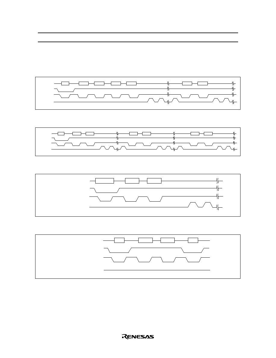
Timing Waveforms
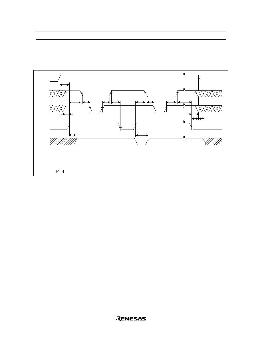
Power on and off Sequence
t
VRS
t
RP
t
CES
t
BSY
t
CEH
t
CESR
t
RP
t
BSY
t
CES
t
CEH
t
VRH
t
DFP
t
CWRH
t
CESR
t
CWRS
V
CC
CE
WE
RES
RDY
/
Busy
*
1
*
2
*
1
High-Z
Ready
Notes: 1.
RES
must be kept at the V
ILR
level referred to DC characteristics at the rising and falling edges of V
CC
to guarantee data stored in the chip.
2.
RES
must be kept at the V
IHR
level referred to DC characteristics while I/O7 outputs the V
OL
level in the
status data polling and RDY/
Busy
outputs the V
OL
level.
3. : Undefined
HN29V102414 Series
26
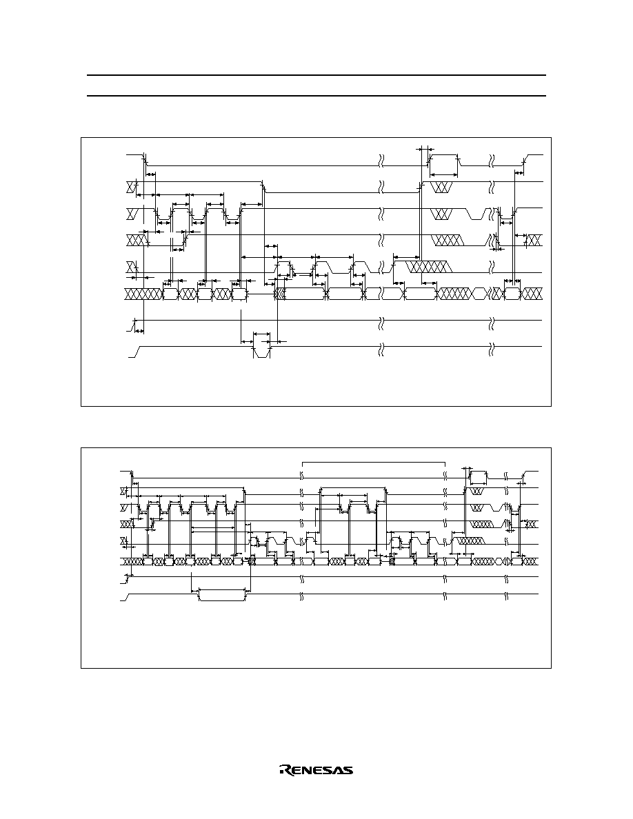
Serial Read (1) (2) Timing Waveform
CE
OE
WE
CDE
RES
t
CES
t
CWC
t
CWC
t
CEH
t
CPH
t
WPH
t
OER
t
WPH
t
WP
t
WP
t
WP
t
SAC
t
SAC
t
SAC
t
SP
t
OES
SC
t
WSD
t
SCC
t
SCC
t
SOH
I/O0 to I/O7
t
SCS
t
DS
t
RP
t
DB
t
RBSY
t
RS
t
AS
t
AS
t
DH
t
DS
t
CDS
t
DF
t
SAC
t
CDH
t
WP
t
COH
t
DH
t
AH
t
AH
t
OEL
High-Z
RDY
/
Busy
D0out/D2048out
D1out/D2049out
D2111out/D2111out
00H
/F0H
SA(1)
Notes: 1. The status returns to the standby at the rising edge of
CE
.
2. Output data is not valid after the number of the SC pulse exceeds 2112 and 64 in the serial read mode (1)and (2), respectively.
3. After any commands are written, the status can return to the standby after the command FFH is input and
CE
turns to the V
IH
level.
t
OEWS
t
CDS
t
CDS
t
CDH
*
2
*
2
*
1
*
3
t
SPL
t
SH
t
SH
FFH
SA(2)
Serial Read (1) with CA before SC Timing Waveform
CE
OE
WE
CDE
RES
t
CES
t
CWC
t
CWC
t
CWC
t
CWC
t
CDS
t
CPH
t
CEH
t
WP
t
CDH
t
WPH
t
WPH
t
OER
t
WPH
t
WPH
t
WP
t
WP
t
WP
t
WP
t
WP
SC
t
SCD
t
WSD
t
SCC
t
SCC
t
SCC
t
SCC
t
OES
t
OES
t
WPH
t
CWC
t
OEWS
I/O0 to I/O7
t
SCS
t
DS
t
AS
t
AS
t
AS
t
AS
t
AH
t
AH
t
AS
t
SH
t
AS
t
AH
t
AH
t
OEL
t
AH
t
AH
t
SH
t
SH
t
SAC
t
SAC
t
SAC
t
SAC
t
DF
t
SP
t
RP
t
RBSY
t
DB
t
RS
t
DH
t
OER
t
WP
t
SW
t
SP
t
SPL
t
WP
t
COH
h-1 cycle
High-Z
RDY
/
Busy
D(n)out
D(n+1)out
D(n+i)out
00H
SA(1)
CA(1)
CA(2)
CA(2)'
CA(1)'
D(m)out
D(m+1)out
D(m+j)out
FFH
Notes: 1. The status returns to the Standby at the rising edge of
CE
.
2. Output data is not valid after the number of the SC pulse exceeds (2112-n). (i
2111-n, 0
n
2111)
3. Output data is not valid after the number of the SC pulse exceeds (2112-m). (j
2111-m, 0
m
2111)
4. After any commands are written, the status can return to the standby after the command FFH is input and
CE
turns
to the V
IH
level.
5. This interval can be repeated (h-1) cycle. (1
h
2048 + 64)
t
OEWS
t
CDS
t
CDS
t
CDH
*
2
*
2
*
3
*
3
*
1
*
5
*
4
t
SOH
t
SOH
t
SPL
t
OEL
t
SAC
t
SAC
t
SAC
t
DF
t
DS
t
DH
t
SAC
t
SH
SA(2)

HN29V102414 Series
27
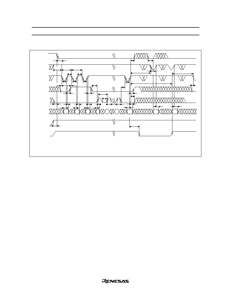
Serial Read (1) with CA after SC Timing Waveform
CE
OE
WE
CDE
RES
t
CES
t
CWC
t
CWC
t
CDS
t
CPH
t
CEH
t
WP
t
CDH
t
WPH
t
WPH
t
OER
t
WP
t
WP
t
WP
SC
t
SCC
t
SCC
t
WSD
t
OES
t
SCC
t
SCC
t
OES
t
OEL
t
WPH
t
CWC
t
OEWS
I/O0 to I/O7
t
SCS
t
DS
t
AS
t
AS
t
SAC
t
SP
t
SH
t
AH
t
AH
t
SH
t
SH
t
SPL
t
SAC
t
SAC
t
SAC
t
DF
t
AH
t
AH
t
AS
t
AS
t
RP
t
DB
t
RBSY
t
RS
t
DH
t
OER
t
WP
t
SW
t
SP
t
SPL
t
WP
t
COH
h cycle
High-Z
RDY
/
Busy
D0out
D1out
D(k)out
00H
SA(1)
CA(2)
CA(1)
D(m)out
D(m+1)out
D(m+j)out
FFH
Notes: 1. The status returns to the Standby at the rising edge of
CE
.
2. Output data is not valid after the number of the SC pulse exceeds 2112. (0
k
2111)
3. Output data is not valid after the number of the SC pulse exceeds (2112-m). (j
2111-m, 0
m
2111)
4. After any commands are written, the status can return to the standby after the command FFH is input and
CE
turns to the V
IH
level.
5. This interval can be repeated h cycle. (1
h
2048 + 64)
t
OEWS
t
CDS
t
CDS
t
CDH
*
2
*
3
*
3
*
1
*
5
*
2
*
4
t
SOH
t
SOH
t
OEL
t
SAC
t
SAC
t
SAC
t
DF
t
DS
t
DH
t
SAC
t
SH
SA(2)
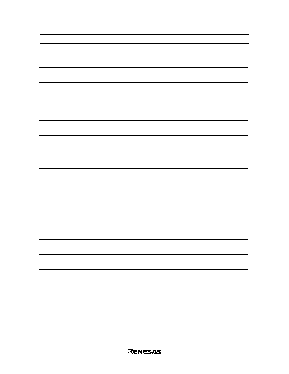
Erase and Status Data Polling Timing Waveform (Sector Erase)
CE
OE
WE
CDE
RES
t
CES
t
CWC
t
CWC
t
CWC
t
CEH
t
OEPS
t
CE
t
OE
t
RDY
t
ASE
t
WPH
t
WPH
t
WPH
t
WP
t
WP
t
WP
t
WP
t
CDH
SC
t
SCHW
I/O0 to I/O7
t
SCS
t
DS
t
DS
t
DB
t
RP
t
AS
t
AS
t
DH
t
DH
t
DF
t
DF
t
CDS
t
AH
t
AH
High-Z
High-Z
RDY
/
Busy
IO7 = V
OH
IO7 = V
OL
20H
SA(1)
SA(2)
Notes: 1. Any commands,including reset command FFH, cannot be input while RDY/
Busy
outputs a V
OL
.
2. The status returns to the standby status after RDY/
Busy
returns to High-Z.
t
OEWS
t
CDS
t
CDS
t
CDS
t
CDH
t
CDH
B0H
*
2
*
1

HN29V102414 Series
28
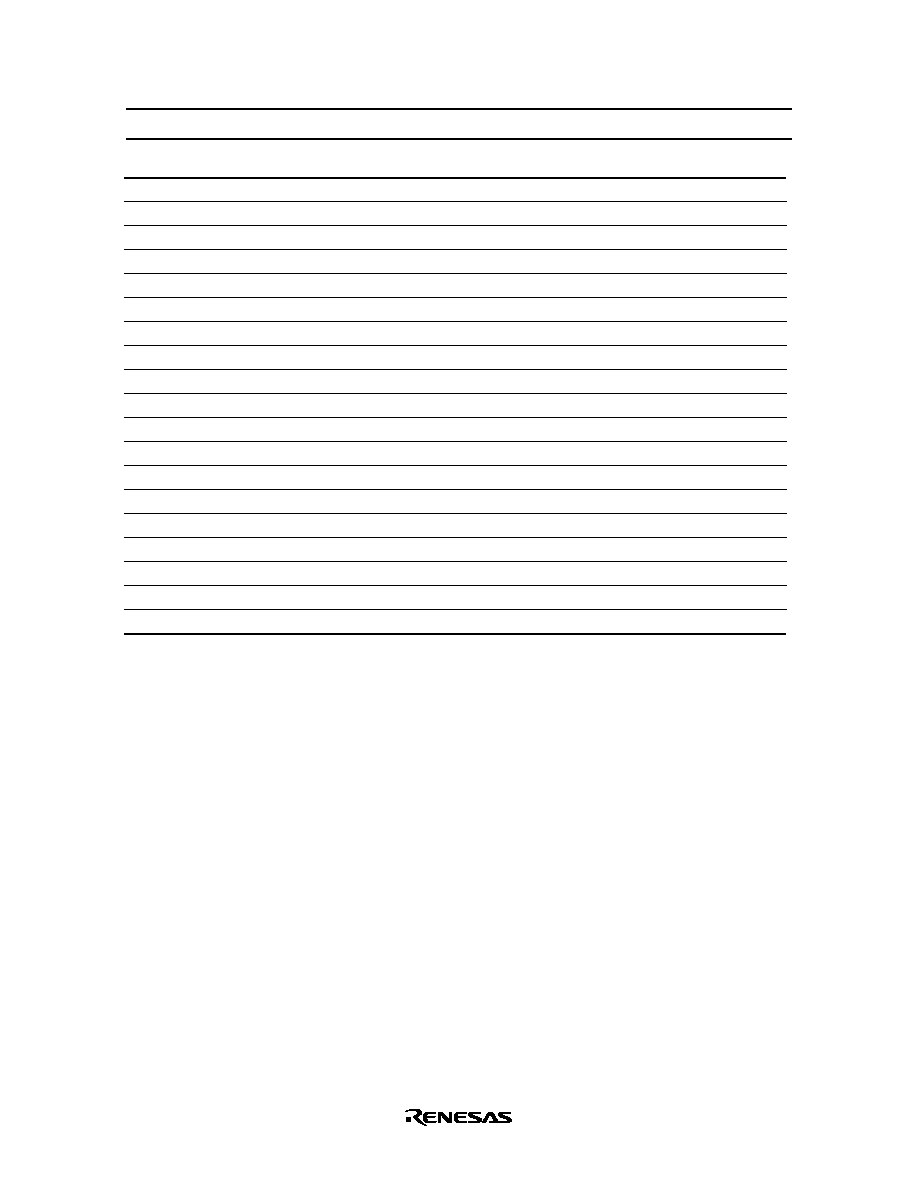
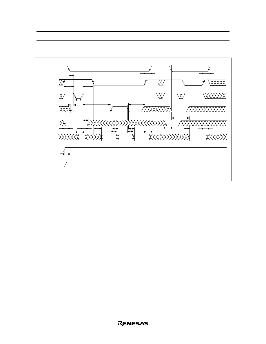
Program (1) and Status Data Polling Timing Waveform
*
1
CE
WE
RES
RDY
/
Busy
OE
CDE
SC
I/O0 to I/O7
t
CES
t
OEWS
t
CWC
t
WPH
t
WP
t
CDS
t
CDS
t
SCS
t
RP
t
CDH
t
DS
t
CDH
t
OE
t
CDSS
t
WP
t
WP
t
SW
t
SCHW
t
CDH
t
WP
t
SPL
t
SCC
t
WPH
t
CEH
t
CE
t
RDY
t
CWC
t
DB
t
OEPS
t
ASP
t
DH
t
AS
t
AS
t
AH
t
SP
t
SP
t
DS
t
DH
40H
10H
PD0
PD1
PD2111
I/O7 = V
OL
I/O7 = V
OH
SA (1)
SA (2)
High-Z
High-Z
*
2
*
3
t
DF
t
DF
t
CDS
Notes: 1. The programming operation is not guranteed when the number of the SC pulse exceeds 2112.
2. Any commands, including reset command FFH, cannot be input while RDY/
Busy
is V
OL
.
3. The status returns to the standby status after RDY/
Busy
returns to High-Z.
4. By using program (1), data can be programmed additionally for each sector before erase.
t
AH
t
SDH
t
SDS

HN29V102414 Series
29
Program (1) with CA before SC and Status Data Polling Timing Waveform
CE
SC
I/O0 to I/O7
RES
RDY
/
Busy
OE
WE
CDE
Notes: 1. The programming operation is not guaranteed when the number of the SC pulse exceeds (2112 ≠ n).(i
2111 ≠ n, 0
n
2111)
2. The programming operation is not guaranteed when the number of the SC pulse exceeds (2112 ≠ m).(j
2111 ≠ m, 0
m
2111)
3. Any commands, including reset command FFH, cannot be input while RDY/
Busy
is V
OL
.
4. The status returns to the standby status after RDY/
Busy
returns to High-Z.
5. By using program (1), data can be programmed additionally for each sector before erase.
6. This interval can be repeated (h ≠ 1) cycle.(1
h
2048 + 64)
t
CES
t
WP
t
CDS
t
CDS
t
CDH
t
CDH
t
CDSS
t
CDH
t
CDSH
t
AS
t
AS
t
SDS
t
DS
t
DB
t
SCC
t
AH
t
AH
t
SDH
t
DH
t
DF
t
DF
t
CDS
t
SW
t
CDSS
t
DS
t
AS
t
AS
t
AS
t
AS
t
SDS
t
DH
t
AH
t
AH
t
AH
t
AH
t
SCS
t
WP
t
RP
t
WP
t
WP
t
WP
t
WP
t
WP
t
WP
t
CEH
t
CE
t
CDH
t
SCHW
t
OEPS
t
RDY
t
OE
t
SW
t
CDS
t
WPH
t
CWC
t
OEWS
t
CWC
t
CWC
t
CWC
t
CWC
t
WPH
t
WPH
t
WPH
t
WPH
High-Z
High-Z*
4
10H
SA(1)
SA(2)
CA(1)
CA(2)
CA(1)'
CA(2)'
PD(n) PD(n+1) PD(n+i)*
1
*
1
*
2
*
3
PD(m) PD(m+1)PD(m+j)*
2
h≠1 cycle*
6
I/O7=V
OL
I/O7=V
OH
t
SDH
t
SPL
t
SP
t
SP
t
SP
t
SP
t
SPL
t
SCC
40H
t
ASP
Program (1) with CA after SC and Status Data Polling Timing Waveform
CE
SC
I/O0 to I/O7
RES
RDY
/
Busy
OE
WE
CDE
Notes: 1. The programming operation is not guaranteed when the number of the SC pulse exceeds 2112.(0
k
2111)
2. The programming operation is not guaranteed when the number of the SC pulse exceeds (2112 ≠ m).(j
2111 ≠ m, 0
m
2111)
3. Any commands, including reset command FFH, cannot be input while RDY/
Busy
is V
OL
.
4. The status returns to the standby status after RDY/
Busy
returns to High-Z.
5. By using program (1), data can be programmed additionally for each sector before erase.
6. This interval can be repeated h cycle.(1
h
2048 + 64)
t
CES
t
WP
t
CDS
t
CDS
t
CDH
t
CDH
t
CDSS
t
CDH
t
CDSH
t
AS
t
AS
t
SDS
t
DS
t
DB
t
SCC
t
AH
t
AH
t
SDH
t
DH
t
DF
t
DF
t
CDS
t
SW
t
CDSS
t
DS
t
AS
t
AS
t
SDS
t
DH
t
AH
t
AH
t
SDH
t
SCS
t
WP
t
RP
t
WP
t
WP
t
WP
t
WP
t
CEH
t
CE
t
CDH
t
SCHW
t
OEPS
t
RDY
t
OE
t
SW
t
CDS
t
WPH
t
CWC
t
OEWS
t
CWC
t
CWC
t
WPH
t
WPH
High-Z
High-Z*
4
10H
SA(1)
SA(2)
PD0
PD1
CA(1)
CA(2)
PD(k)*
1
*
1
*
2
*
3
PD(m) PD(m+1)PD(m+j)*
2
h cycle*
6
I/O7=V
OL
I/O7=V
OH
t
SPL
t
SP
t
SP
t
SP
t
SP
t
SPL
t
SCC
40H
t
ASP
HN29V102414 Series
30
Program (2) and Status Data Polling Timing Waveform
*
1
CE
WE
RES
RDY
/
Busy
OE
CDE
SC
I/O0 to I/O7
t
CES
t
OEWS
t
CWC
t
WPH
t
WP
t
CDS
t
CDS
t
SCS
t
RP
t
CDH
t
DS
t
CDH
t
OE
t
CDSS
t
WP
t
WP
t
SW
t
SCHW
t
CDH
t
WP
t
SPL
t
SCC
t
WPH
t
CEH
t
CDS
t
CE
t
RDY
t
CWC
t
DB
t
OEPS
t
ASP
t
DH
t
AS
t
AS
t
AH
t
SP
t
SP
t
DS
t
DH
40H
1FH
PD0
PD1
PD2111
I/O7 = V
OL
I/O7 = V
OH
SA (1)
SA (2)
High-Z
High-Z
*
2
*
3
t
DF
t
DF
Notes: 1. The programming operation is not guranteed when the number of the SC pulse exceeds 2112.
2. Any commands, including reset command FFH, cannot be input while RDY/
Busy
is V
OL
.
3. The status returns to the standby status after RDY/
Busy
returns to High-Z.
4. By using program (2), the programmed data of each sector must be erased before programming next data.
t
AH
t
SDH
t
SDS

HN29V102414 Series
31
Program (3) and Status Data Polling Timing Waveform
*
1
CE
WE
RES
RDY
/
Busy
OE
CDE
SC
I/O0 to I/O7
t
CES
t
OEWS
t
CWC
t
WPH
t
WP
t
CDS
t
CDS
t
SCS
t
RP
t
CDH
t
DS
t
CDH
t
OE
t
CDSS
t
WP
t
WP
t
SW
t
SCHW
t
CDH
t
WP
t
SPL
t
SCC
t
CEH
t
CDS
t
CE
t
RDY
t
CWC
t
DB
t
OEPS
t
ASP
t
DH
t
AS
t
AS
t
AH
t
SP
t
SP
t
DS
t
DH
40H
0FH
PD2048 PD2049 PD2111
I/O7 = V
OL
I/O7 = V
OH
SA (1)
SA (2)
High-Z
High-Z
*
2
*
3
t
DF
t
DF
Notes: 1. The programming operation is not guranteed when the number of the SC pulse exceeds 64.
2. Any commands, including reset command FFH, cannot be input while RDY/
Busy
is V
OL
.
3. The status returns to the standby status after RDY/
Busy
returns to High-Z.
4. By using program (3), the data can be programmed additionally for each sector before erase.
t
AH
t
SDH
t
SDS

HN29V102414 Series
32
Program (4) and Status Data Polling Timing Waveform
*
1
CE
WE
RES
RDY
/
Busy
OE
CDE
SC
I/O0 to I/O7
t
CES
t
OEWS
t
CWC
t
WPH
t
WP
t
CDS
t
CDS
t
SCS
t
RP
t
DB
t
DB
t
RS
t
RBSY
t
CDH
t
DS
t
CDH
t
WSD
t
OE
t
CDSS
t
WP
t
WP
t
SW
t
SCHW
t
CDH
t
CDS
t
WP
t
SPL
t
SCC
t
WPH
t
CEH
t
CE
t
RDY
t
CWC
t
DB
t
OEPS
t
ASP
t
DH
t
AS
t
AS
t
AH
t
SP
t
SP
t
DS
t
DH
40H
11H
PD0
PD1
PD2111
I/O7 = V
OL
I/O7 = V
OH
SA (1)
SA (2)
High-Z
High-Z
*
2
*
3
t
DF
t
DF
Notes: 1. The programming operation is not guranteed when the number of the SC pulse exceeds 2112.
2. Any commands, including reset command FFH, cannot be input while RDY/
Busy
is V
OL
.
3. The status returns to the standby status after RDY/
Busy
returns to High-Z.
4. By using program (4), data can be rewritten for each sector.
t
AH
t
SDH
t
SDS

HN29V102414 Series
33
Program (4) with CA before SC and Status Data Polling Timing Waveform
CE
SC
I/O0 to I/O7
RES
RDY
/
Busy
OE
WE
CDE
Notes: 1. The programming operation is not guaranteed when the number of the SC pulse exceeds (2112 ≠ n).(i
2111 ≠ n, 0
n
2111)
2. The programming operation is not guaranteed when the number of the SC pulse exceeds (2112 ≠ m).(j
2111 ≠ m, 0
m
2111)
3. Any commands, including reset command FFH, cannot be input while RDY/
Busy
is V
OL
.
4. The status returns to the standby status after RDY/
Busy
returns to High-Z.
5. By using program (4), data can be rewritten for each sector.
6. This interval can be repeated (h ≠ 1) cycle.(1
h
2048 + 64)
t
CES
t
WP
t
CDS
t
CDS
t
CDH
t
CDH
t
WSD
t
CDSS
t
CDH
t
CDSH
t
AS
t
AS
t
SDS
t
DS
t
DB
t
SCC
t
AH
t
AH
t
SDH
t
DH
t
DF
t
DF
t
CDS
t
SW
t
CDSS
t
DS
t
AS
t
AS
t
AS
t
AS
t
SDS
t
DH
t
AH
t
AH
t
AH
t
AH
t
SCS
t
WP
t
RP
t
DB
t
RBSY
t
RS
t
WP
t
WP
t
WP
t
WP
t
WP
t
WP
t
CEH
t
CE
t
CDH
t
SCHW
t
OEPS
t
RDY
t
OE
t
SW
t
CDS
t
WPH
t
CWC
t
OEWS
t
CWC
t
CWC
t
CWC
t
CWC
t
WPH
t
WPH
t
WPH
t
WPH
High-Z
High-Z*
4
11H
SA(1)
CA(1)
CA(2)
CA(1)'
CA(2)'
PD(n+1) PD(n+i)*
1
*
1
*
2
*
3
PD(m) PD(m+1)PD(m+j)*
2
h≠1 cycle*
6
I/O7=V
OL
I/O7=V
OH
t
SDH
t
SPL
t
SP
t
SP
t
SP
t
SP
t
SPL
t
SCC
40H
SA(2)
PD(n)
t
ASP
Program (4) with CA after SC and Status Data Polling Timing Waveform
CE
SC
I/O0 to I/O7
RES
RDY
/
Busy
OE
WE
CDE
Notes: 1. The programming operation is not guaranteed when the number of the SC pulse exceeds 2112.(0
k
2111)
2. The programming operation is not guaranteed when the number of the SC pulse exceeds (2112 ≠ m).(j
2111 ≠ m, 0
m
2111)
3. Any commands, including reset command FFH, cannot be input while RDY/
Busy
is V
OL
.
4. The status returns to the standby status after RDY/
Busy
returns to High-Z.
5. By using program (4), data can be rewritten for each sector.
6. This interval can be repeated h cycle.(1
h
2048 + 64)
t
CES
t
WP
t
CDS
t
CDS
t
CDH
t
CDH
t
WSD
t
CDSS
t
CDH
t
CDSH
t
AS
t
AS
t
SDS
t
DS
t
DB
t
SCC
t
AH
t
AH
t
SDH
t
DH
t
DF
t
DF
t
CDS
t
SW
t
CDSS
t
DS
t
AS
t
AS
t
SDS
t
DH
t
AH
t
AH
t
SDH
t
SCS
t
WP
t
RP
t
DB
t
RS
t
RBSY
t
WP
t
WP
t
WP
t
WP
t
CEH
t
CE
t
CDH
t
SCHW
t
OEPS
t
RDY
t
OE
t
SW
t
CDS
t
WPH
t
CWC
t
OEWS
t
CWC
t
CWC
t
WPH
t
WPH
High-Z
High-Z*
4
11H
SA(1)
PD1
CA(1)
CA(2)
PD(k)*
1
*
1
*
2
*
3
PD(m) PD(m+1)PD(m+j)*
2
h cycle*
6
I/O7=V
OL
I/O7=V
OH
t
SPL
t
SP
t
SP
t
SP
t
SP
t
SPL
t
SCC
40H
SA(2)
PD0
t
ASP
HN29V102414 Series
34
ID and Status Register Read Timing Waveform
CE
OE
WE
CDE
RES
t
CES
t
CE
t
COH
t
COH
t
WP
t
SCHW
SC
I/O0 to I/O7
t
SCS
t
DH
t
DF
t
OE
t
SCS
t
OE
t
CDAC
t
CDAC
t
CDF
t
CDF
t
RP
t
DF
High-Z
RDY
/
Busy
Status
register
90H
Manufacturer
code
Manufacturer
code
Device
code
Note: 1. The status returns to the standby at the rising edge of
CE
.
t
OEWS
t
OEPS
t
CDH
t
CDOH
t
CDS
*
1
*
1
t
DS

HN29V102414 Series
35
Data Recovery Read Timing Waveform
CE
OE
WE
CDE
RES
t
CES
t
CPH
t
COH
t
CEH
t
WP
t
WP
t
CDH
t
SCC
t
SP
t
SAC
t
SAC
t
SCC
t
SOH
SC
I/O0 to I/O7
t
SCS
t
OEL
t
OES
t
CDS
t
DS
t
DH
High-Z
High
RDY
/
Busy
01H
FFH
D0out
D1out
D2111out
Notes: 1. The status returns to the standby at the rising edge of
CE
.
2. Output data is not valid after the number of the SC pulse exceed 2112 in the recovery data read mode.
3. After any commands are written, the status can turns to the standby after the command FFH is input
and
CE
turns to the V
IH
level.
t
OEWS
t
OER
t
SH
t
SH
t
SAC
t
SAC
t
CDS
*
3
*
1
*
2
*
2
t
DS
t
CDH
t
DH
t
SPL
t
DF

HN29V102414 Series
36
Data Recovery Write Timing Waveform
CE
OE
WE
CDE
RES
t
CES
t
CWC
t
CWC
t
CWC
t
CEH
t
OEPS
t
ASP
t
CE
t
OE
t
RDY
t
WPH
t
WPH
t
WPH
t
WP
t
WP
t
WP
t
WP
t
CDH
SC
t
SCHW
I/O0 to I/O7
t
SCS
t
DS
t
DS
t
DB
t
AS
t
AS
t
DH
t
DH
t
DF
t
DF
t
CDS
t
AH
t
AH
High-Z
High
High-Z
RDY
/
Busy
IO7 = V
OH
IO7 = V
OL
12H
SA(1)
SA(2)
Notes: 1. Any commands,including reset command FFH, cannot be input while RDY/
Busy
is V
OL
.
2. The status returns to the standby status after RDY/
Busy
returns to High-Z.
t
OEWS
t
CDS
t
CDS
t
CDS
t
CDH
t
CDH
*
2
*
1
40H

HN29V102414 Series
37
Clear Status Register Timing Waveform
WE
CDE
RES
RDY
/
Busy
SC
I/O0 to I/O7
OE
CE
t
CES
t
CDS
t
SCS
t
DS
t
DH
t
WP
t
CDH
t
WPH
t
CEH
t
CDS
t
CDH
t
WP
t
CPH
t
CES
t
CDH
t
WP
t
SCS
t
DS
t
DH
tDS
tDH
High-Z
Note 1. The status returns to the standby at the rising edge of
CE
.
*
1
Next
Command
Next
Command
50H
t
OEWS
High
t
OEWS
t
CDS

HN29V102414 Series
38
Function Description
Status Register: The HN29V102414 outputs the operation status data as follows: I/O7 pin outputs a V
OL
to
indicate that the memory is in either erase or program operation. The level of I/O7 pin turns to a V
OH
when
the operation finishes. I/O5 and I/O4 pins output V
OL
s to indicate that the erase and program operations
complete in a finite time, respectively. If these pins output V
OH
s, it indicates that these operations have timed
out. If I/O6 pin outputs V
OH
, it indicates a possibility that can be corrected by ECC, choose data correction by
ECC or not by reading out the data. When these pins monitor, I/O7 pin must turn to a V
OH
. To execute other
erase and program operation, the status data must be cleared after a time out occurs. From I/O0 to I/O3 pins
are reserved for future use. The pins output V
OL
s and should be masked out during the status data read mode.
The function of the status register is summarized in the following table.
I/O
Flag definition
Definition
I/O7
Ready/
Busy
V
OH
= Ready, V
OL
= Busy
I/O6
Program/Erase ECC
check
When I/O7 outputs V
OH
, V
OH
= ECC available, V
OL
= ECC not available.
I/O5
Erase check
V
OH
= Fail, V
OL
= Pass
I/O4
Program check
V
OH
= Fail, V
OL
= Pass
I/O3
Reserved
Outputs a V
OL
and should be masked out during the status data poling mode.
I/O2
Reserved
I/O1
Reserved
I/O0
Reserved
ECC Applicability
I/O7
I/O6
I/O5
I/O4
System data correction by ECC
V
OH
V
OH
V
OH
V
OL
Needed
V
OH
V
OL
V
OH
V
OL
Not needed. Sector replacement
V
OH
V
OH
V
OL
V
OH
Needed
V
OH
V
OL
V
OL
V
OH
Not needed. Sector replacement
This device needs to be corrected failure data by ECC on system or Spare sectors, by reading out again the
failure sector data when program/erase error occures.

HN29V102414 Series
39
Requirement for System
Specifications
Program/Erase Endurance: 10
5
cycles
Item
Min
Typ
Max
Unit
Usable sectors (initially)
64,226
--
65,536
sector
Spare sectors (1-chip operation)
579
--
--
sector
(2-chip operation)
1158
--
--
sector
ECC (Error Correction Code)
3
--
--
bit/sector

HN29V102414 Series
40
Unusable Sector
Initially, the HN29V102414 includes unusable sectors. The unusable sectors must be distinguished from the
usable sectors by the system as follows.
1. Check the partial invalid sectors in the devices on the system. The usable sectors were programmed the
following data. Refer to the flowchart "Indication of unusable sectors".
Initial Data of Usable Sectors
Column address
0H to 81FH
820H
821H
822H
823H
824H
825H
826H to 83FH
Data
FFH
1CH
71H
C7H
1CH
71H
C7H
FFH
2. Do not erase and program to the partial invalid sectors by the system.
Sector number = 0
Read data
Bad sector*
2
Sector number =
Sector number + 1
Column address = 820H to 825H
Yes
Yes
No
No
Check data*
1
Sector number = 32,767
START
END
Notes: 1. Refer to table "Initial data of usable sectors".
2. Bad sectors are installed in system.
The Unusable Sector Indication Flow (1-chip)

HN29V102414 Series
41
Requirements for High System Reliability
The device may fail during a program, erase or read operation due to write or erase cycles. The following
architecture will enable high system reliability if a failure occurs.
1. For an error in read operation: An ECC (Error Correction Code) or a similar function which can correct
3-bits per each sectors is required for data reliability. When error occurs, data must not be corrected by
replacing to spare sector.
2. For errors in program or erase operations: The device may fail during a program or erase operation due to
write or erase cycles. The status register indicates if the erase and program operation complete in a finite
time. When an error occured in the sector, try to reprogram the data into another sector. Avoid further
system access to the sector that error happens. Typically, recommended number of a spare sectors are
1.8% (579 sectors/chip (min)) of initial usable 32,113 sectors/chip (min.) by each device. For the
reprogramming, do not use the data from the failed sectors, because the data from the failed sectors are not
fixed. So the reprogram data must be the data reloaded from the external buffer, or use the Data recovery
read mode or the Data recovery write mode (see the "Mode Description" and under figure "Spare Sector
Replacement Flow after Program Error"). To avoid consecutive sector failures, choose addresses of spare
sectors as far as possible from the failed sectors. In this case, 10
5
cycles of program/erase endurance is
guaranteed.

HN29V102414 Series
42
Program start
Program end
Clear status register
Program start
Program end
Load data from
external buffer
Data recovery read
Data recovery write
Check RDY/
Busy
Set an usable sector
Check RDY/
Busy
Set another
usable sector
Yes
No
Check status
Check status: Status register read
Yes
No
Check status
START
END
Spare Sector Replacement Flow after Program Error
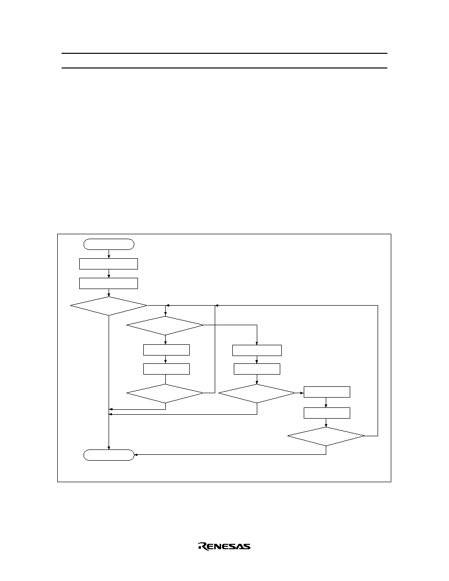
HN29V102414 Series
43
For Errors in program or erase operations
The device may fail during a program or erase operation. Failure mode can be confirmed by read out the
status register after complete the erase and program operations. There are two failure modes specified by
each codes:
1: Status register error flag: I/O6 = V
OL
Replace sector under the "Spare Sectors Replacement Flow at Status Register I/O6 Read". Replacement must
be applied to one sector(2k bytes) which contains failure bits.
2: Status register error flag: I/O6 = V
OH
Escape the program data temporary under the "Replacement Flow at Status Register I/O6 Read". If failure
data can be corrected by ECC, do not replace to spare sector. If failure data can not be corrected by ECC,
replace to spare sector. Replacement must be applied to one sector(2k bytes) which contains failure bits.
Program start
Program end
Sector Replacement
Sector Replacement
Program end
Program end
Check RDY/
Busy
Set an usable sector
Yes
Yes
Yes
No
No
Check status
Yes
No
Check status
Check status
Check ECC
Check I/O6
START
END
Escape program deta*
1
Read error sector
V
OL
V
OH
Note: 1. Refer to 'Spare sector replacement flow after program error' to escape the deta.
Check status: Status register read
Check I/O6: I/O6 output monitor
Check ECC: Correct by ECC?
No
Spare Sectors Replacement Flow at Status Register I/O6 Read

HN29V102414 Series
44
Memory Structure
32,768 sectors
sector
2,112 bytes (16,896 bits)
byte (8 bits)
bit
Bit: Minimum unit of data.
Byte: Input/output data unit in programming and reading. (1 byte = 8 bits)
Sector: Page unit in erase, programming and reading. (1 sector = 2,112 bytes = 16,896 bits)
Device: 1 device = 32,768 sectors.
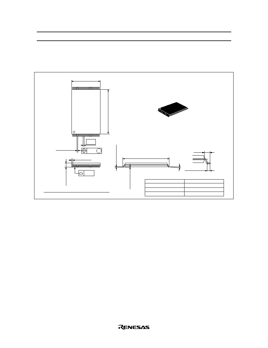
HN29V102414 Series
45
Package Dimensions
HN29V102414T Series (TFP-48DA)
0.08
0.08
M
0.50
12.00
*0.22
±
0.08
20.00
±
0.20
0.05
±
0.05
1.20 Max
18.40
0
∞
≠ 8
∞
48
1
24
25
12.40 Max
0.45 Max
*0.17
±
0.05
0.50
±
0.10
0.80
0.20
±
0.06
0.125
±
0.04
Hitachi Code
JEDEC
EIAJ
Mass (reference value)
TFP-48DA
Conforms
Conforms
0.52 g
Unit: mm
*Dimension including the plating thickness
Base material dimension
HN29V102414 Series
46
Cautions
1. Hitachi neither warrants nor grants licenses of any rights of Hitachi's or any third party's patent,
copyright, trademark, or other intellectual property rights for information contained in this document.
Hitachi bears no responsibility for problems that may arise with third party's rights, including intellectual
property rights, in connection with use of the information contained in this document.
2. Products and product specifications may be subject to change without notice. Confirm that you have
received the latest product standards or specifications before final design, purchase or use.
3. Hitachi makes every attempt to ensure that its products are of high quality and reliability. However,
contact Hitachi's sales office before using the product in an application that demands especially high
quality and reliability or where its failure or malfunction may directly threaten human life or cause risk of
bodily injury, such as aerospace, aeronautics, nuclear power, combustion control, transportation, traffic,
safety equipment or medical equipment for life support.
4. Design your application so that the product is used within the ranges guaranteed by Hitachi particularly for
maximum rating, operating supply voltage range, heat radiation characteristics, installation conditions and
other characteristics. Hitachi bears no responsibility for failure or damage when used beyond the
guaranteed ranges. Even within the guaranteed ranges, consider normally foreseeable failure rates or
failure modes in semiconductor devices and employ systemic measures such as fail-safes, so that the
equipment incorporating Hitachi product does not cause bodily injury, fire or other consequential damage
due to operation of the Hitachi product.
5. This product is not designed to be radiation resistant.
6. No one is permitted to reproduce or duplicate, in any form, the whole or part of this document without
written approval from Hitachi.
7. Contact Hitachi's sales office for any questions regarding this document or Hitachi semiconductor
products.
Hitachi, Ltd.
Semiconductor & Integrated Circuits
Nippon Bldg., 2-6-2, Ohte-machi, Chiyoda-ku, Tokyo 100-0004, Japan
Tel: (03) 3270-2111 Fax: (03) 3270-5109
Copyright © Hitachi, Ltd., 2001. All rights reserved. Printed in Japan.
Hitachi Asia Ltd.
Hitachi Tower
16 Collyer Quay #20-00
Singapore 049318
Tel : <65>-538-6533/538-8577
Fax : <65>-538-6933/538-3877
URL : http://semiconductor.hitachi.com.sg
URL
http://www.hitachisemiconductor.com/
Hitachi Asia Ltd.
(Taipei Branch Office)
4/F, No. 167, Tun Hwa North Road
Hung-Kuo Building
Taipei (105), Taiwan
Tel : <886>-(2)-2718-3666
Fax : <886>-(2)-2718-8180
Telex : 23222 HAS-TP
URL : http://www.hitachi.com.tw
Hitachi Asia (Hong Kong) Ltd.
Group III (Electronic Components)
7/F., North Tower
World Finance Centre,
Harbour City, Canton Road
Tsim Sha Tsui, Kowloon Hong Kong
Tel : <852>-(2)-735-9218
Fax : <852>-(2)-730-0281
URL : http://semiconductor.hitachi.com.hk
Hitachi Europe GmbH
Electronic Components Group
Dornacher Straþe 3
D-85622 Feldkirchen
Postfach 201,D-85619 Feldkirchen
Germany
Tel: <49> (89) 9 9180-0
Fax: <49> (89) 9 29 30 00
Hitachi Europe Ltd.
Electronic Components Group
Whitebrook Park
Lower Cookham Road
Maidenhead
Berkshire SL6 8YA, United Kingdom
Tel: <44> (1628) 585000
Fax: <44> (1628) 585200
Hitachi Semiconductor
(America) Inc.
179 East Tasman Drive
San Jose,CA 95134
Tel: <1> (408) 433-1990
Fax: <1>(408) 433-0223
For further information write to:
Colophon 5.0