
Rev.2.00, Jan.11.2005, page 1 of 20
HN58X2432SI/HN58X2464SI
Two-wire serial interface
32k EEPROM (4-kword
◊
8-bit)/64k EEPROM (8-kword
◊
8-bit)
REJ03C0135-0200
Rev.2.00
Jan.11.2005
Description
HN58X2432SI, HN58X2464SI are two-wire serial interface EEPROM (Electrically Erasable and
Programmable ROM). They realize high speed, low power consumption and a high level of reliability by
employing advanced MNOS memory technology and CMOS process and low voltage circuitry technology.
They also have a 32-byte page programming function to make their write operation faster.
Note: Renesas Technology's serial EEPROM are authorized for using consumer applications such as
cellular phone, camcorders, audio equipment. Therefore, please contact Renesas Technology's
sales office before using industrial applications such as automotive systems, embedded controllers,
and meters.
Features
∑ Single supply: 1.8 V to 5.5 V
∑ Two-wire serial interface (I
2
C
TM
serial bus*
1
)
∑ Clock frequency: 400 kHz
∑ Power dissipation:
Standby: 3 µA (max)
Active (Read): 1 mA (max)
Active (Write): 3 mA (max)
∑ Automatic page write: 32-byte/page
∑ Write cycle time: 10 ms (2.7 V to 5.5 V)/15ms (1.8 V to 2.7 V)
∑ Endurance: 10
5
Cycles (Page write mode)
∑ Data retention: 10 Years
HN58X2432SI/HN58X2464SI
Rev.2.00, Jan.11.2005, page 2 of 20
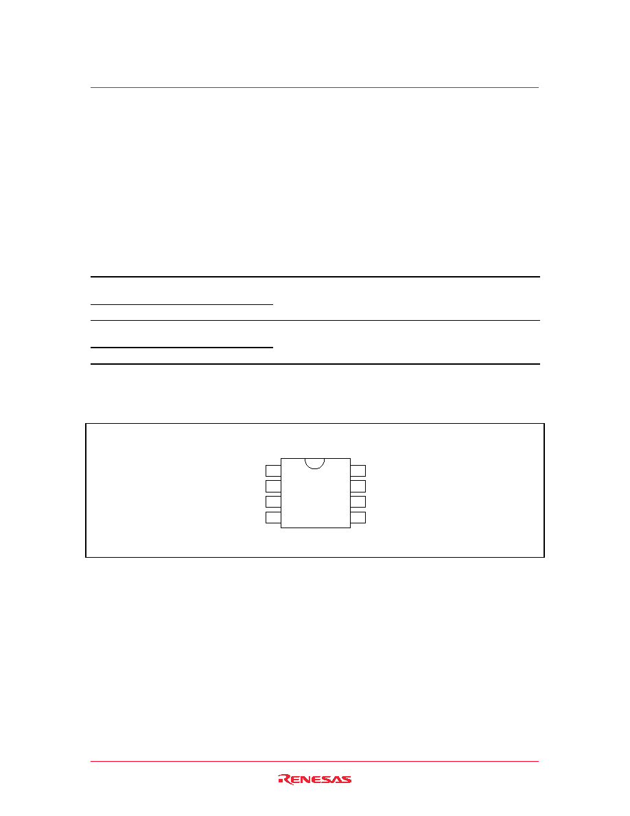
∑ Small size packages: TSSOP-8pin, SOP-8pin
∑ Shipping tape and reel
TSSOP 8-pin: 3,000 IC/reel
SOP 8-pin: 2,500 IC/reel
∑ Temperature range: -40 to +85∞C
∑ Lead free products.
Note: 1. I
2
C is a trademark of Philips Corporation.
Ordering Information
Type No.
Internal organization Operating voltage Frequency Package
HN58X2432SFPIE 32k bit (4096
◊
8-bit) 1.8 V to 5.5 V
400 kHz
150 mil 8-pin plastic SOP
(FP-8DBV)
HN58X2464SFPIE 64k bit (8192
◊
8-bit)
Lead free
HN58X2432STIE
32k bit (4096
◊
8-bit) 1.8 V to 5.5 V
400 kHz
8-pin plastic TSSOP
(TTP-8DAV)
HN58X2464STIE
64k bit (8192
◊
8-bit)
Lead free
Pin Arrangement
1
2
3
4
8
7
6
5
A0
A1
A2
V
SS
V
CC
WP
SCL
SDA
(Top view)
8-pin TSSOP
8-pin SOP

HN58X2432SI/HN58X2464SI
Rev.2.00, Jan.11.2005, page 3 of 20
Pin Description
Pin name
Function
A0 to A2
Device address
SCL
Serial clock input
SDA
Serial data input/output
WP Write
protect
V
CC
Power
supply
V
SS
Ground
Block Diagram
Control
logic
High voltage generator
Address generator
X decoder
Y decoder
Memory array
Y-select & Sense amp.
Serial-parallel converter
V
CC
V
SS
WP
A0, A1, A2
SCL
SDA
Absolute Maximum Ratings
Parameter Symbol
Value
Unit
Supply voltage relative to V
SS
V
CC
-
0.6 to +7.0
V
Input voltage relative to V
SS
Vin
-
0.5
*
2
to +7.0
*
3
V
Operating temperature range
*
1
Topr
-
40 to +85
∞
C
Storage temperature range
Tstg
-
65 to +125
∞
C
Notes: 1. Including electrical characteristics and data retention.
2. Vin (min):
-
3.0 V for pulse width
50 ns.
3. Should not exceed V
CC
+ 1.0 V.
HN58X2432SI/HN58X2464SI
Rev.2.00, Jan.11.2005, page 4 of 20
DC Operating Conditions
Parameter Symbol
Min
Typ
Max
Unit
Supply voltage
V
CC
1.8
5.5 V
V
SS
0 0 0 V
Input high voltage
V
IH
V
CC
◊
0.7
V
CC
+ 1.0
V
Input low voltage
V
IL
≠0.3
*
1
V
CC
◊
0.3
V
Operating temperature
Topr
-
40
+85
∞
C
Note: 1. V
IL
(min):
-
1.0 V for pulse width
50 ns.
DC Characteristics
(Ta =
-
40 to +85
∞
C, V
CC
= 1.8 V to 5.5 V)
Parameter
Symbol
Min Typ Max Unit Test
conditions
Input leakage current
I
LI
2.0
µ
A V
CC
= 5.5 V, Vin = 0 to 5.5 V
(SCL, SDA)
I
LI
20
µ
A V
CC
= 5.5 V, Vin = 0 to 5.5 V
(A0 to A2, WP)
Output leakage current
I
LO
2.0
µ
A V
CC
= 5.5 V, Vout = 0 to 5.5 V
Standby V
CC
current
I
SB
1.0
3.0
µA
Vin = V
SS
or V
CC
Read V
CC
current
I
CC1
1.0 mA V
CC
= 5.5 V, Read at 400 kHz
Write V
CC
current
I
CC2
3.0 mA V
CC
= 5.5 V, Write at 400 kHz
Output low voltage
V
OL2
0.4 V V
CC
= 4.5 to 5.5 V, I
OL
= 1.6 mA
V
CC
= 2.7 to 4.5 V, I
OL
= 0.8 mA
V
CC
= 1.8 to 2.7 V, I
OL
= 0.4 mA
V
OL1
0.2 V V
CC
= 1.8 to 2.7 V, I
OL
= 0.2 mA
Capacitance
(Ta = +25
∞
C, f = 1 MHz)
Parameter
Symbol
Min
Typ
Max
Unit
Test
conditions
Input capacitance (A0 to A2, SCL, WP) Cin
*
1
6.0
pF
Vin = 0 V
Output capacitance (SDA)
C
I/O
*
1
6.0
pF
Vout = 0 V
Note: 1. This parameter is sampled and not 100
%
tested.

HN58X2432SI/HN58X2464SI
Rev.2.00, Jan.11.2005, page 5 of 20
AC Characteristics
(Ta =
-
40 to +85
∞
C, V
CC
= 1.8 to 5.5 V)
Test Conditions
∑ Input pules levels:
V
IL
= 0.2
◊ V
CC
V
IH
= 0.8
◊ V
CC
∑ Input rise and fall time: 20 ns
∑ Input and output timing reference levels: 0.5 ◊ V
CC
∑ Output load: TTL Gate + 100 pF
Parameter Symbol
Min
Typ
Max
Unit
Notes
Clock frequency
f
SCL
400
kHz
Clock pulse width low
t
LOW
1200
ns
Clock pulse width high
t
HIGH
600
ns
Noise suppression time
t
I
50 ns 1
Access time
t
AA
100
900
ns
Bus free time for next mode
t
BUF
1200
ns
Start hold time
t
HD.STA
600
ns
Start setup time
t
SU.STA
600
ns
Data in hold time
V
CC
= 3.0 V to 5.5 V
t
HD.DAT
10
ns
V
CC
= 1.8 V to 3.0 V
t
HD.DAT
20
ns
Data in setup time
t
SU.DAT
100
ns
Input rise time
t
R
300
ns 1
Input fall time
t
F
300
ns 1
Stop setup time
t
SU.STO
600
ns
Data out hold time
t
DH
50
ns
Write protect hold time
t
HD.WP
1200
ns
Write protect setup time
t
SU.WP
0
ns
Write cycle time
V
CC
= 2.7 V to 5.5 V
t
WC
10 ms 2
V
CC
= 1.8 V to 2.7 V
t
WC
15 ms 2
Notes: 1. This parameter is sampled and not 100
%
tested.
2.
t
WC
is the time from a stop condition to the end of internally controlled write cycle.