Rev.1.00, Mar.12.2004, page 1 of 13
R1RP0416D Series
4M High Speed SRAM (256-kword
◊
16-bit)
REJ03C0108-0100Z
Rev. 1.00
Mar.12.2004
Description
The R1RP0416D Series is a 4-Mbit high speed static RAM organized 256-k word
◊
16-bit. It has realized
high speed access time by employing CMOS process (6-transistor memory cell) and high speed circuit
designing technology. It is most appropriate for the application which requires high speed, high density
memory and wide bit width configuration, such as cache and buffer memory in system. It is packaged in
400-mil 44-pin plastic SOJ and 400-mil 44-pin plastic TSOPII.
Features
∑
Single 5.0 V supply: 5.0 V
±
10%
∑
Access time: 12 ns (max)
∑
Completely static memory
No clock or timing strobe required
∑
Equal access and cycle times
∑
Directly TTL compatible
All inputs and outputs
∑
Operating current: 160 mA (max)
∑
TTL standby current: 40 mA (max)
∑
CMOS standby current : 5 mA (max)
: 1.0 mA (max) (L-version)
∑
Data retention current: 0.5 mA (max) (L-version)
∑
Data retention voltage: 2 V (min) (L-version)
∑
Center V
CC
and V
SS
type pin out
Ordering Information
Type No.
Access time
Package
R1RP0416DGE-2PR
12 ns
400-mil 44-pin plastic SOJ (44P0K)
R1RP0416DGE-2LR 12
ns
R1RP0416DSB-2PR
12 ns
400-mil 44-pin plastic TSOPII (44P3W-H)
R1RP0416DSB-2LR 12
ns
R1RP0416D Series
Rev.1.00, Mar.12.2004, page 2 of 13
Pin Arrangement
A0
A1
A2
A3
A4
CS#
I/O1
I/O2
I/O3
I/O4
V
CC
V
SS
I/O5
I/O6
I/O7
I/O8
WE#
A5
A6
A7
A8
A9
(Top View)
1
2
3
4
5
6
7
8
9
10
11
12
13
14
15
16
17
18
19
20
21
22
44
43
42
41
40
39
38
37
36
35
34
33
32
31
30
29
28
27
26
25
24
23
A17
A16
A15
OE#
UB#
LB#
I/O16
I/O15
I/O14
I/O13
V
SS
V
CC
I/O12
I/O11
I/O10
I/O9
NC
A14
A13
A12
A11
A10
44-pin SOJ
1
2
3
4
5
6
7
8
9
10
11
12
13
14
15
16
17
18
19
20
21
22
A0
A1
A2
A3
A4
CS#
I/O1
I/O2
I/O3
I/O4
V
CC
V
SS
I/O5
I/O6
I/O7
I/O8
WE#
A5
A6
A7
A8
A9
A17
A16
A15
OE#
UB#
LB#
I/O16
I/O15
I/O14
I/O13
V
SS
V
CC
I/O12
I/O11
I/O10
I/O9
NC
A14
A13
A12
A11
A10
44
43
42
41
40
39
38
37
36
35
34
33
32
31
30
29
28
27
26
25
24
23
44-pin TSOP
(Top View)
Pin Description
Pin name
Function
A0 to A17
Address input
I/O1 to I/O16
Data input/output
CS# Chip
select
OE# Output
enable
WE# Write
enable
UB#
Upper byte select
LB#
Lower byte select
V
CC
Power supply
V
SS
Ground
NC
No connection
R1RP0416D Series
Rev.1.00, Mar.12.2004, page 3 of 13
Block Diagram
1024-row
◊
32-column
◊
8-block
◊
16-bit
(4,194,304 bits)
CS
V
CC
V
SS
A8 A9 A17 A15 A16 A0 A2 A4
Column I/O
Column decoder
I/O1
WE#
Input
data
control
Row
decoder
OE#
CS#
CS
CS
LB#
UB#
I/O16
I/O9
I/O8
.
.
.
.
.
.
A14
A13
A12
A5
A6
A7
A11
A10
A3
A1
(LSB)
(MSB)
Internal
voltage
generator
(LSB)
(MSB)
R1RP0416D Series
Rev.1.00, Mar.12.2004, page 4 of 13
Operation Table
CS# OE# WE# LB# UB# Mode
V
CC
current
I/O1
-
-
-
-
I/O8 I/O9
-
-
-
-
I/O16 Ref.
cycle
H
◊
◊
◊
◊
Standby
I
SB
, I
SB1
High-Z High-Z
L H H
◊
◊
Output
disable
I
CC
High-Z
High-Z
L L H L L Read
I
CC
Output Output Read
cycle
L L H L H Lower
byte
read
I
CC
Output High-Z Read
cycle
L L H H L Upper
byte
read
I
CC
High-Z Output Read
cycle
L L H H H
I
CC
High-Z
High-Z
L
◊
L L L Write
I
CC
Input Input Write
cycle
L
◊
L L H Lower
byte
write I
CC
Input
High-Z
Write
cycle
L
◊
L H L Upper
byte
write I
CC
High-Z
Input
Write
cycle
L
◊
L H H
I
CC
High-Z
High-Z
Note: H: V
IH
, L: V
IL
,
◊
: V
IH
or V
IL
Absolute Maximum Ratings
Parameter Symbol
Value
Unit
Supply voltage relative to V
SS
V
CC
-
0.5 to +7.0
V
Voltage on any pin relative to V
SS
V
T
-
0.5
*
1
to V
CC
+ 0.5
*
2
V
Power dissipation
P
T
1.0
W
Operating temperature
Topr
0 to +70
∞
C
Storage temperature
Tstg
-
55 to +125
∞
C
Storage temperature under bias
Tbias
-
10 to +85
∞
C
Notes: 1. V
T
(min) =
-
2.0 V for pulse width (under shoot)
6 ns.
2.
V
T
(max) = V
CC
+ 2.0 V for pulse width (over shoot)
6 ns.
Recommended DC Operating Conditions
(Ta = 0 to +70
∞
C)
Parameter Symbol
Min
Typ
Max
Unit
Supply voltage
V
CC
*
3
4.5 5.0 5.5 V
V
SS
*
4
0 0 0 V
Input voltage
V
IH
2.2
V
CC
+ 0.5
*
2
V
V
IL
-
0.5
*
1
0.8 V
Notes: 1. V
IL
(min) =
-
2.0 V for pulse width (under shoot)
6 ns.
2.
V
IH
(max) = V
CC
+ 2.0 V for pulse width (over shoot)
6 ns.
3. The supply voltage with all V
CC
pins must be on the same level.
4. The supply voltage with all V
SS
pins must be on the same level.
R1RP0416D Series
Rev.1.00, Mar.12.2004, page 5 of 13
DC Characteristics
(Ta = 0 to +70
∞
C, V
CC
= 5.0 V
±
10%, V
SS
= 0 V)
Parameter
Symbol
Min Max Unit Test
conditions
Input leakage current
|I
LI
|
2
µ
A V
IN
= V
SS
to V
CC
Output leakage current
|I
LO
|
2
µ
A V
IN
= V
SS
to V
CC
Operation power supply current
I
CC
160
mA
Min
cycle
CS# = V
IL
, l
OUT
= 0 mA
Other inputs = V
IH
/V
IL
Standby power supply current
I
SB
40
mA
Min cycle, CS# = V
IH
,
Other inputs = V
IH
/V
IL
I
SB1
5
mA
f = 0 MHz
V
CC
CS#
V
CC
-
0.2 V,
(1) 0 V
V
IN
0.2 V or
(2) V
CC
V
IN
V
CC
-
0.2 V
*
1
1.0
*
1
Output voltage
V
OL
0.4 V I
OL
= 8 mA
V
OH
2.4
V I
OH
=
-
4 mA
Note: 1. This characteristics is guaranteed only for L-version.
Capacitance
(Ta = +25
∞
C, f = 1.0 MHz)
Parameter Symbol
Min
Max
Unit
Test
conditions
Input capacitance
*
1
C
IN
6 pF V
IN
= 0 V
Input/output capacitance
*
1
C
I/O
8 pF V
I/O
= 0 V
Note: 1. This parameter is sampled and not 100% tested.
R1RP0416D Series
Rev.1.00, Mar.12.2004, page 6 of 13
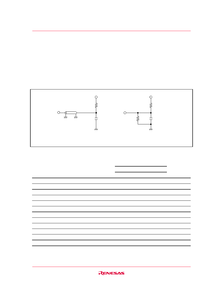
AC Characteristics
(Ta = 0 to +70
∞
C, V
CC
= 5.0 V
±
10%, unless otherwise noted.)
Test Conditions
∑
Input pulse levels: 3.0 V/0.0 V
∑
Input rise and fall time: 3 ns
∑
Input and output timing reference levels: 1.5 V
∑
Output load: See figures (Including scope and jig)
Output load (B)
(for t
CLZ
, t
OLZ
, t
BLZ
, t
CHZ
, t
OHZ
,
t
BHZ
, t
WHZ
, and t
OW
)
D
OUT
255
480
5 V
5 pF
1.5 V
30 pF
D
OUT
RL = 50
Output load (A)
Zo = 50
Read Cycle
R1RP0416D
-2
Parameter Symbol
Min
Max
Unit
Notes
Read cycle time
t
RC
12
ns
Address access time
t
AA
12 ns
Chip select access time
t
ACS
12 ns
Output enable to output valid
t
OE
6 ns
Byte select to output valid
t
BA
6 ns
Output hold from address change
t
OH
3
ns
Chip select to output in low-Z
t
CLZ
3
ns
1
Output enable to output in low-Z
t
OLZ
0
ns
1
Byte select to output in low-Z
t
BLZ
0
ns
1
Chip deselect to output in high-Z
t
CHZ
6 ns
1
Output disable to output in high-Z
t
OHZ
6 ns
1
Byte deselect to output in high-Z
t
BHZ
6 ns
1
R1RP0416D Series
Rev.1.00, Mar.12.2004, page 7 of 13
Write Cycle
R1RP0416D
-2
Parameter Symbol
Min
Max
Unit
Notes
Write cycle time
t
WC
12
ns
Address valid to end of write
t
AW
8
ns
Chip select to end of write
t
CW
8
ns
8
Write pulse width
t
WP
8
ns
7
Byte select to end of write
t
BW
8
ns
Address setup time
t
AS
0
ns
5
Write recovery time
t
WR
0
ns
6
Data to write time overlap
t
DW
6
ns
Data hold from write time
t
DH
0
ns
Write disable to output in low-Z
t
OW
3
ns
1
Output disable to output in high-Z
t
OHZ
6 ns
1
Write enable to output in high-Z
t
WHZ
6 ns
1
Notes: 1. Transition is measured
±
200 mV from steady voltage with output load (B). This parameter is
sampled and not 100% tested.
2. If the CS# or LB# or UB# low transition occurs simultaneously with the WE# low transition or
after the WE# transition, output remains a high impedance state.
3. WE# and/or CS# must be high during address transition time.
4. If CS#, OE#, LB# and UB# are low during this period, I/O pins are in the output state. Then the
data input signals of opposite phase to the outputs must not be applied to them.
5.
t
AS
is measured from the latest address transition to the latest of CS#, WE#, LB# or UB# going
low.
6.
t
WR
is measured from the earliest of CS#, WE#, LB# or UB# going high to the first address
transition.
7. A write occurs during the overlap of a low CS#, a low WE# and a low LB# or a low UB# (t
WP
). A
write begins at the latest transition among CS# going low, WE# going low and LB# going low or
UB# going low. A write ends at the earliest transition among CS# going high, WE# going high
and LB# going high or UB# going high.
8.
t
CW
is measured from the later of CS# going low to the end of write.
R1RP0416D Series
Rev.1.00, Mar.12.2004, page 8 of 13
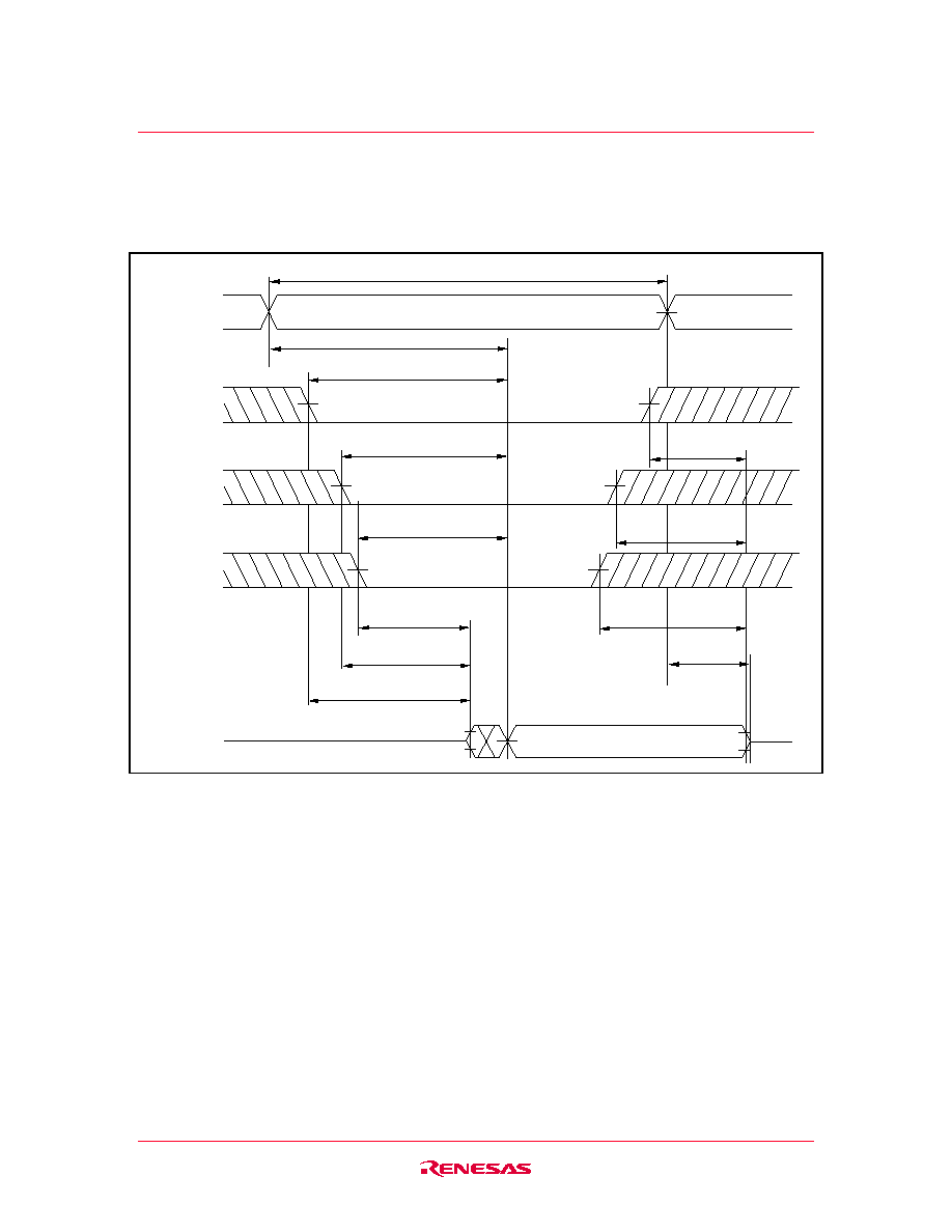
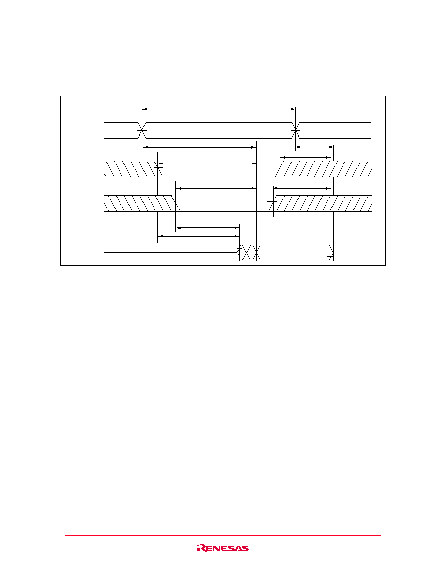
Timing Waveforms
Read Timing Waveform (1) (WE# = V
IH
)
t
AA
t
ACS
t
OE
t
BA
t
BLZ
t
OLZ
t
CLZ
t
OH
t
CHZ
t
OHZ
t
BHZ
t
RC
Address
Valid address
Valid data
D
OUT
CS#
OE#
LB#, UB#
High impedance
*
1
*
1
*
1
*
1
*
1
*
1
*
4
*
4
R1RP0416D Series
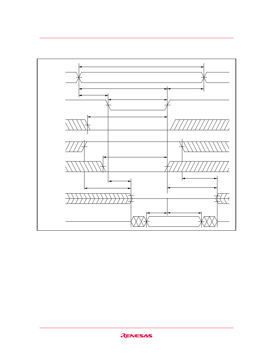
Rev.1.00, Mar.12.2004, page 9 of 13
Read Timing Waveform (2) (WE# = V
IH
, LB# = V
IL
, UB# = V
IL
)
t
AA
t
ACS
t
RC
t
OE
t
CLZ
Valid data
Address
CS#
D
OUT
Valid address
High impedance
t
OHZ
OE#
t
OH
t
CHZ
t
OLZ
*
1
*
1
*
1
*
1
*
4
*
4
R1RP0416D Series
Rev.1.00, Mar.12.2004, page 10 of 13
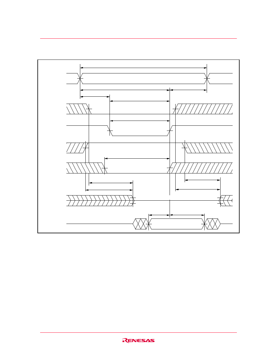
Write Timing Waveform (1) (WE# Controlled)
Address
WE#
*
3
t
WC
t
AW
t
AS
t
WR
t
WP
t
WHZ
t
OLZ
t
OW
t
OHZ
t
CW
t
BW
t
DH
t
DW
Valid address
Valid data
CS#
*
3
OE#
LB#, UB#
D
OUT
D
IN
High impedance
*
2
R1RP0416D Series
Rev.1.00, Mar.12.2004, page 11 of 13
Write Timing Waveform (2) (CS# Controlled)
Address
CS#
*
3
t
WC
t
AW
t
AS
t
WR
t
WP
t
WHZ
t
OLZ
t
OW
t
OHZ
t
CW
t
BW
t
DH
t
DW
Valid address
Valid data
WE#
*
3
OE#
LB#, UB#
D
OUT
D
IN
High impedance
*
2
*
4
R1RP0416D Series
Rev.1.00, Mar.12.2004, page 12 of 13
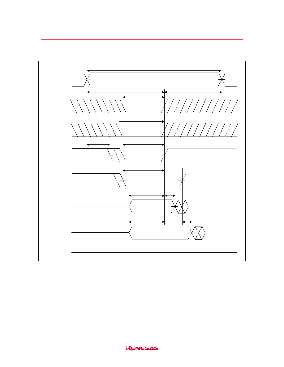
Write Timing Waveform (3) (LB#, UB# Controlled, OE# = V
IH
)
Address
D
IN
-UB
(D
IN
-LB)
D
IN
-LB
(D
IN
-UB)
D
OUT
High impedance
Valid address
t
DW
t
DH
t
CW
t
AS
t
BW
t
WP
t
WC
t
WR
t
AW
WE#
*
3
CS#
*
3
UB# (LB#)
LB# (UB#)
t
BW
Valid data
t
DW
t
DH
Valid data
R1RP0416D Series
Rev.1.00, Mar.12.2004, page 13 of 13
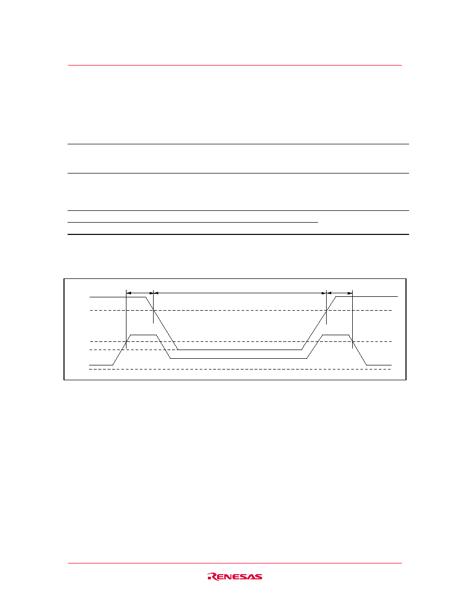
Low V
CC
Data Retention Characteristics
(Ta = 0 to +70
∞
C)
This characteristics is guaranteed only for L-version.
Parameter
Symbol
Min Max Unit Test
conditions
V
CC
for data retention
V
DR
2.0
V V
CC
CS#
V
CC
-
0.2 V,
(1) 0 V
V
IN
0.2 V or
(2) V
CC
V
IN
V
CC
-
0.2 V
Data retention current
I
CCDR
500
µ
A V
CC
= 3 V
V
CC
CS#
V
CC
-
0.2 V,
(1) 0 V
V
IN
0.2 V or
(2) V
CC
V
IN
V
CC
-
0.2 V
Chip deselect to data retention time
t
CDR
0
ns
See retention waveform
Operation recovery time
t
R
5
ms
Low V
CC
Data Retention Timing Waveform
CC
V
2.2 V
4.5 V
0 V
CS#
t
CDR
t
R
DR
V
Data retention mode
V
CC
CS#
V
CC
-
0.2 V

Revision History
R1RP0416D Series Data Sheet
Contents of Modification
Rev. Date
Page Description
0.01 Sep. 30, 2003
Initial
issue
1.00 Mar.12.2004
Deletion of Preliminary
Keep safety first in your circuit designs!
1. Renesas Technology Corp. puts the maximum effort into making semiconductor products better and more reliable, but there is always the possibility that trouble
may occur with them. Trouble with semiconductors may lead to personal injury, fire or property damage.
Remember to give due consideration to safety when making your circuit designs, with appropriate measures such as (i) placement of substitutive, auxiliary
circuits, (ii) use of nonflammable material or (iii) prevention against any malfunction or mishap.
Notes regarding these materials
1. These materials are intended as a reference to assist our customers in the selection of the Renesas Technology Corp. product best suited to the customer's
application; they do not convey any license under any intellectual property rights, or any other rights, belonging to Renesas Technology Corp. or a third party.
2. Renesas Technology Corp. assumes no responsibility for any damage, or infringement of any third-party's rights, originating in the use of any product data,
diagrams, charts, programs, algorithms, or circuit application examples contained in these materials.
3. All information contained in these materials, including product data, diagrams, charts, programs and algorithms represents information on products at the time of
publication of these materials, and are subject to change by Renesas Technology Corp. without notice due to product improvements or other reasons. It is
therefore recommended that customers contact Renesas Technology Corp. or an authorized Renesas Technology Corp. product distributor for the latest product
information before purchasing a product listed herein.
The information described here may contain technical inaccuracies or typographical errors.
Renesas Technology Corp. assumes no responsibility for any damage, liability, or other loss rising from these inaccuracies or errors.
Please also pay attention to information published by Renesas Technology Corp. by various means, including the Renesas Technology Corp. Semiconductor
home page (http://www.renesas.com).
4. When using any or all of the information contained in these materials, including product data, diagrams, charts, programs, and algorithms, please be sure to
evaluate all information as a total system before making a final decision on the applicability of the information and products. Renesas Technology Corp. assumes
no responsibility for any damage, liability or other loss resulting from the information contained herein.
5. Renesas Technology Corp. semiconductors are not designed or manufactured for use in a device or system that is used under circumstances in which human life
is potentially at stake. Please contact Renesas Technology Corp. or an authorized Renesas Technology Corp. product distributor when considering the use of a
product contained herein for any specific purposes, such as apparatus or systems for transportation, vehicular, medical, aerospace, nuclear, or undersea repeater
use.
6. The prior written approval of Renesas Technology Corp. is necessary to reprint or reproduce in whole or in part these materials.
7. If these products or technologies are subject to the Japanese export control restrictions, they must be exported under a license from the Japanese government and
cannot be imported into a country other than the approved destination.
Any diversion or reexport contrary to the export control laws and regulations of Japan and/or the country of destination is prohibited.
8. Please contact Renesas Technology Corp. for further details on these materials or the products contained therein.
Sales Strategic Planning Div. Nippon Bldg., 2-6-2, Ohte-machi, Chiyoda-ku, Tokyo 100-0004, Japan
http://www.renesas.com
Renesas Technology America, Inc.
450 Holger Way, San Jose, CA 95134-1368, U.S.A
Tel: <1> (408) 382-7500 Fax: <1> (408) 382-7501
Renesas Technology Europe Limited.
Dukes Meadow, Millboard Road, Bourne End, Buckinghamshire, SL8 5FH, United Kingdom
Tel: <44> (1628) 585 100, Fax: <44> (1628) 585 900
Renesas Technology Europe GmbH
Dornacher Str. 3, D-85622 Feldkirchen, Germany
Tel: <49> (89) 380 70 0, Fax: <49> (89) 929 30 11
Renesas Technology Hong Kong Ltd.
7/F., North Tower, World Finance Centre, Harbour City, Canton Road, Hong Kong
Tel: <852> 2265-6688, Fax: <852> 2375-6836
Renesas Technology Taiwan Co., Ltd.
FL 10, #99, Fu-Hsing N. Rd., Taipei, Taiwan
Tel: <886> (2) 2715-2888, Fax: <886> (2) 2713-2999
Renesas Technology (Shanghai) Co., Ltd.
26/F., Ruijin Building, No.205 Maoming Road (S), Shanghai 200020, China
Tel: <86> (21) 6472-1001, Fax: <86> (21) 6415-2952
Renesas Technology Singapore Pte. Ltd.
1, Harbour Front Avenue, #06-10, Keppel Bay Tower, Singapore 098632
Tel: <65> 6213-0200, Fax: <65> 6278-8001
RENESAS SALES OFFICES
© 2003, 2004. Renesas Technology Corp., All rights reserved. Printed in Japan.
Colophon .1.0