 | –≠–ª–µ–∫—Ç—Ä–æ–Ω–Ω—ã–π –∫–æ–º–ø–æ–Ω–µ–Ω—Ç: DR3300 | –°–∫–∞—á–∞—Ç—å:  PDF PDF  ZIP ZIP |

Æ
RF Monolithics, Inc.
Phone: (972) 233-2903
Fax: (972) 387-8148
E-mail: info@rfm.com
Page 1 of 5
RFM Europe
Phone: 44 1963 251383
Fax: 44 1963 251510
http://www.rfm.com
©1999 by RF Monolithics, Inc. The stylized RFM logo are registered trademarks of RF Monolithics, Inc.
DR3300-060304
Electrical Characteristics, 115.2 kbps Amplitude-Shift Keyed
Characteristic
Sym
Notes
Minimum
Typical
Maximum
Units
Operating Frequency
f
O
916.25
916.75
MHz
Modulation Type
ASK
Data Rate
1
Mbps
Receiver Performance (ASK @ 1 Mbps)
Input Current, 3 Vdc Supply
I
R
4.8
mA
Input Signal for 10
-4
BER, 25 ∞C
-76
dBm
Rejection, ±30 MHz
R
REJ
55
dB
Transmitter Performance (ASK @ 1 Mbps)
Peak Input Current, 3 Vdc Supply
I
TP
12
mA
Peak Output Power
P
O
0.75
mW
Turn On/Turn Off Time
t
ON
/t
OFF
0.2/0.2
µs
Sleep to Receive Switch Time (15 ms sleep, -70 dBm signal)
t
SR
10
µs
Sleep Mode Current
I
S
0.75
µA
Transmit to Receive Switch Time (15 ms transmit, -70 dBm signal)
t
TOR
10
µs
Receive to Transmit Switch Time
t
RTO
12
µs
Power Supply Voltage Range
Vcc
2.7
3.5
Vdc
Operating Ambient Temperature
T
A
-40
+85
∞C
∑
Designed for Short-Range Wireless Data Communications
∑
Supports 1 Mbps Encoded Data Transmissions
∑
3 V, Low Current Operation plus Sleep Mode
∑
Ready to Use OEM Module
The DR3300 transceiver module is ideal for short-range wireless data applications where robust operation,
small size and low power consumption are required. The DR3300 utilizes RFM's TR1100 amplifier-
sequenced hybrid (ASH) architecture to achieve this unique blend of characteristics. The receiver section of
the TR1100 is sensitive and stable. A wide dynamic range log detector provides robust performance in the
presence of on-channel interference or noise. Two stages of SAW filtering provide excellent receiver out-of-
band rejection. The TR1100 transmitter is optimized amplitude-shift keyed (ASK) modulation at data rates up
to 1 Mbps. The transmitter employs SAW filtering to suppress output harmonics, facilitating compliance with
FCC 15.249 and similar regulations. The DR3300 includes the TR1100 plus most configuration components
in a ready-to-use PCB assembly, excellent for prototyping and intermediate volume production runs.
Absolute Maximum Ratings
Rating
Value
Units
Power Supply and All Input/Output Pins
-0.3 to +4.0
V
Non-Operating Case Temperature
-50 to +100
∞C
Soldering Temperature (10 seconds)
230
∞C
916.50 MHz
Transceiver
Module
DR3300

916.50 MHz Transceiver Module
RF Monolithics, Inc.
Phone: (972) 233-2903
Fax: (972) 387-8148
E-mail: info@rfm.com
Page 2 of 5
RFM Europe
Phone: 44 1963 251383
Fax: 44 1963 251510
http://www.rfm.com
©1999 by RF Monolithics, Inc. The stylized RFM logo are registered trademarks of RF Monolithics, Inc.
DR3300-060304
R3
R4
R8
R1
R2
R6
R5
C3
L2
C1
L1
C4
C5
+
ASH Transceiver
20
1
11
10
CTR0 (12)
CTR1 (11)
VCC (9)
LPF ADJ (8)
GND (6, 7, 10)
RFIO
(13)
RF GND
(14)
AGC/VCC
(1)
PK DET
(2)
RX BBO
(3)
RX DATA
(4)
TX IN
(5)
DR3300 Schematic
C6
C2
L3
.70
.25
.20
.165
.70
.10
DR3300 Outline Drawing
Dimensions in inches
DR3300 Pin Out
RF
GND
RFIO
AGC/VCC
PK DET
TX IN
RX BBO
RX DATA
CTR0
CTR1
GND
VCC
LPF ADJ
1
2
3
4
5
8
9
10
11
12
13
14
6
7
GND
GND
916.50 MHz Transceiver Module
RF Monolithics, Inc.
Phone: (972) 233-2903
Fax: (972) 387-8148
E-mail: info@rfm.com
Page 3 of 5
RFM Europe
Phone: 44 1963 251383
Fax: 44 1963 251510
http://www.rfm.com
©1999 by RF Monolithics, Inc. The stylized RFM logo are registered trademarks of RF Monolithics, Inc.
DR3300-060304
Pin Descriptions
Pin
Name
Description
1
AGC/VCC
This pin is connected directly to the transceiver AGCCAP pin, which controls the AGC reset operation. To enable AGC oper-
ation (required for ASK transmission) an external capacitor is placed between this pin and ground. The capacitor sets the
minimum time the AGC will hold-in once it is engaged. The hold-in time is set to avoid AGC chattering. For a given hold-in
time t
AGH
, the capacitor value C
AGC
is:
C
AGC
= 19.1* t
AGH
, where t
AGH
is in µs and C
AGC
is in pF
For 1 Mbps operation, a 100 pF ±10% ceramic capacitor should be used at this pin. The value of C
AGC
given above provides
a hold-in time between t
AGH
and 2.65* t
AGH
, depending on operating voltage, temperature, etc. The hold-in time is chosen to
allow the AGC to ride through the longest run of zero bits that can occur in a received data stream. The AGC hold-in time can
be greater than the peak detector decay time, as discussed below. However, the AGC hold-in time should not be set too
long, or the receiver will be slow in returning to full sensitivity once the AGC is engaged by noise or interference. AGC oper-
ation also depends on a functioning peak detector, as discussed below. The AGC capacitor is discharged in the transceiver
power-down (sleep) mode and in the transmit modes.
2
PK DET
This pin is connected directly to the transceiver PKDET pin. This pin controls the peak detector operation. An external capac-
itor between this pin and ground sets the peak detector attack and decay times, which have a fixed 1:1000 ratio. For 1 Mbps
applications, the attack time constant should be set to 0.024 µs with a 100 pF capacitor to ground. (This adequately matches
the peak detector decay time constant of 24 µs to the time constant of the 270 pF coupling capacitor C3.) A ±10% ceramic
capacitor should be used at this pin. The peak detector is used to drive the "dB-below-peak" data slicer and the AGC release
function. The AGC hold-in time can be extended beyond the peak detector decay time with the AGC capacitor, as discussed
above. The peak detector capacitor is discharged in the transceiver power-down (sleep) mode and in the transmit modes.
See the description of Pin 3 below for further information.
3
RX BBO
This pin is connected directly to the transceiver BBOUT pin. On the circuit board, BBOUT also drives the transceiver CMPIN
pin through C3, a 270 pF coupling capacitor (t
BBC
= 17.3 µs). RX BBO can also be used to drive an external data recovery
process (DSP, etc.). The nominal output impedance of this pin is 1 K. The RX BBO signal changes about 10 mV/dB, with a
peak-to-peak signal level of up to 675 mV. The signal at RX BBO is riding on a 1.1 Vdc value that varies somewhat with sup-
ply voltage and temperature, so it should be coupled through a capacitor to an external load. A load impedance of 50 K to
500 K in parallel with no more than 10 pF is recommended. Note the AGC reset function is driven by the signal applied to
CMPIN through C3. When the transceiver is in power-down (sleep) or in a transmit mode, the output impedance of this pin
becomes very high, preserving the charge on the coupling capacitor(s). The value of C3 on the circuit board has been cho-
sen to match typical data encoding schemes at 1 Mbps. If C3 is modified to support different data rates and/or encoding
schemes, make the value of the peak detector capacitor about 1/3 the value of C3.
4
RX DATA
RX DATA is connected directly to the transceiver data output pin, RXDATA. This pin will drive a 10 pF, 500 K parallel load.
The peak current available from this pin increases with the receiver low-pass filter cutoff frequency. In the power-down
(sleep) or transmit modes, this pin becomes high impedance. If required, a 1000 K pull-up or pull-down resistor can be used
to establish a definite logic state when this pin is high impedance (do not connect the pull-up resistor to a supply voltage
higher than 3.5 Vdc or the transceiver will be damaged). This pin must be buffered to successfully drive low-impedance
loads.
5
TX IN
The TX IN pin is connected to the transceiver TXMOD pin through a 4.7 K resistor on the circuit board. Additional series
resistance will often be required between the modulation source and the TX IN pin, depending on the desired output power
and peak modulation voltage (3.3 K typical for a peak modulation voltage of 3 volts). Saturated output power requires about
450 µA of drive current. Peak output power P
O
for a 3 Vdc supply is approximately:
P
O
= 4.8*((V
TXH
≠ 0.9)/(R
M
+ 4.7))
2
, where P
O
is in mW, peak modulation voltage V
TXH
is in volts and external modulation
resistor R
M
is in kilohms
This pin must be held low in the receive and sleep modes. Please refer to section 2.9 of the ASH Transceiver Designer's
Guide for additional information.
6
GND
This is a ground pin.
7
GND
This is a ground pin.
916.50 MHz Transceiver Module
RF Monolithics, Inc.
Phone: (972) 233-2903
Fax: (972) 387-8148
E-mail: info@rfm.com
Page 4 of 5
RFM Europe
Phone: 44 1963 251383
Fax: 44 1963 251510
http://www.rfm.com
©1999 by RF Monolithics, Inc. The stylized RFM logo are registered trademarks of RF Monolithics, Inc.
DR3300-060304
8
LPF ADJ
This pin is the receiver low-pass filter bandwidth adjust, and is connected directly to the transceiver LPFADJ pin. R6 on the
circuit board (1 K) is connected between LPFADJ and ground, and sets the receiver bandwidth for typical 1 Mbps operation.
The filter bandwidth can be increased by adding an external resistor in parallel with R6. The equivalent resistor value can
range from 1 K to 820 ohms, providing a filter 3 dB bandwidth f
LPF
from 1.5 to 1.8 MHz. The 3 dB filter bandwidth is deter-
mined by:
f
LPF
= 1445/(1*R
LPF
/(1 + R
LPF
)), where R
LPF
is in kilohms, and f
LPF
is in kHz
A ±5% resistor should be used to set the filter bandwidth. This will provide a 3 dB filter bandwidth between f
LPF
and 1.3* f
LPF
with variations in supply voltage, temperature, etc. The filter provides a three-pole, 0.05 degree equiripple phase response.
The peak drive current available from RXDATA increases in proportion to the filter bandwidth setting. Refer to sections 1.4.3,
2.5.1 and 2.6.1 in the
ASH Transceiver Designer's Guide for additional information on data rate adjustments.
9
VCC
This is the positive supply voltage pin for the module. The operating voltage range is 2.7 to 3.5 Vdc. It is also possible to use
Pin 1 as the Vcc input. Please refer to the Pin 1 description above.
10
GND
This is a ground pin.
11
CTR1
CTR1 is connected to the CNTRL1 control pin on the transceiver. CTR1 and CTR0 select the transceiver operating modes.
CTR1 and CTR0 both high place the unit in the receive mode. CTR1 and CTR0 both low place the unit in the power-down
(sleep) mode. CTR1 high and CTR0 low place the unit in the ASK transmit mode. CTR1 low and CTR0 high place the unit in
the OOK transmit mode (not used at 115.2 kbps). CTR1 is a high-impedance input (CMOS compatible). This pin must be
held at a logic level; it cannot be left unconnected. At turn on, the voltage on this pin and CTR0 should rise with VCC until
VCC reaches 2.7 Vdc (receive mode). Thereafter, any mode can be selected.
12
CTR0
CTR0 is connected to the CNTRL0 control pin on the transceiver CTR0 is used with CTR1 to control the operating modes of
the transceiver. CTR0 is a high-impedance input (CMOS compatible). This pin must be held at a logic level; it cannot be left
unconnected. At turn on, the voltage on this pin and CTR1 should rise with VCC until VCC reaches 2.7 Vdc (receive mode).
Thereafter, any mode can be selected.
13
RFIO
RFIO is the RF input/output pin. A matching circuit for a 50 ohm load (antenna) is implemented on the circuit board between
this pin and the transceiver SAW filter transducer.
14
RF GND
This pin is the RF ground (return) to be used in conjunction with the RFIO pin. For example, when connecting the transceiver
module to an external antenna, the coaxial cable ground is connected this pin and the coaxial cable center conductor is con-
nected to RFIO.
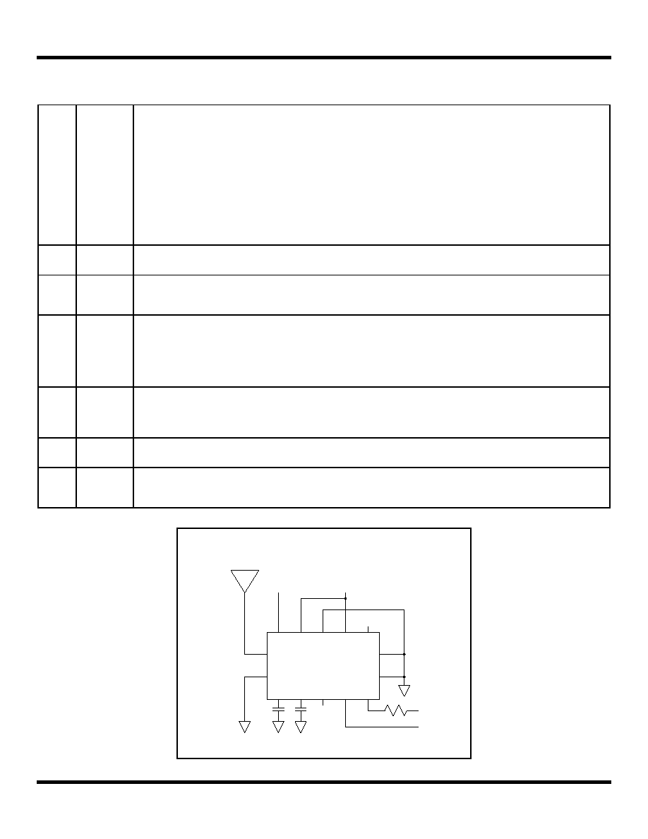
Data In
Data Out
3 Vdc
R/T
1 Mbps Application Circuit
3.3 K
1
2
3
4
5
6
7
8
9
10
11
12
DR3300
100 pF
100 pF
13
14

916.50 MHz Transceiver Module
RF Monolithics, Inc.
Phone: (972) 233-2903
Fax: (972) 387-8148
E-mail: info@rfm.com
Page 5 of 5
RFM Europe
Phone: 44 1963 251383
Fax: 44 1963 251510
http://www.rfm.com
©1999 by RF Monolithics, Inc. The stylized RFM logo are registered trademarks of RF Monolithics, Inc.
DR3300-060304
Item
Reference
Description
Value
Quanitity
1
U1
TR1100 ASH Transceiver
916.50 MHz
1
2
C1, C4, C6
Capacitor SMT 0603
100 pF ±10%
3
3
C2
Capacitor SMT 0603
6.8 pF ±10%
1
4
C3
Capacitor SMT 0603
270 pF ±10%
1
5
C5
Capacitor E1A-B 0805
4.7 µF ±10%
1
6
R1
Resistor Chip 0603
1 M ±5%
1
7
R2
Resistor Chip 0603
11 K ±5%
1
8
R3
Resistor Chip 0603
27 K ±1%
1
9
R4, R8
Resistor Chip 0603
100 K ±1%
2
10
R5
Resistor Chip 0603
4.7 K ±5%
1
11
R6
Resistor Chip 0603
1 K ±5%
1
12
L1
Inductor Chip 0603
18 nH ±5%
1
13
L2
Inductor Chip 0603
100 nH ±10%
1
14
L3
Fair-Rite Chip 0603
2506033017YO
1
15
PCB
Printed Circuit Board ArtWork
AW400-1508-004x1
1
-
R7
Not Used
N/A
0
Note: Preliminary specitications, subject to change without notice.
DR3300 Bill of Materials
8
C2