 | –≠–ª–µ–∫—Ç—Ä–æ–Ω–Ω—ã–π –∫–æ–º–ø–æ–Ω–µ–Ω—Ç: TR3100 | –°–∫–∞—á–∞—Ç—å:  PDF PDF  ZIP ZIP |

1
Æ
TR3100
Rating
Value
Units
Power Supply and All Input/Output Pins
-0.3 to +4.0
V
Non-Operating Case Temperature
-50 to +100
o
C
Soldering Temperature (10 seconds)
250
o
C
Absolute Maximum Ratings
Characteristic
Sym
Notes
Minimum
Typical
Maximum
Units
Operating Frequency
f
O
433.72
434.12
MHz
Modulation Type
ASK
Data Rate
576
kbps
Receiver Performance, High Sensitivity Mode
Sensitivity, 230.4 kbps, 10-3 BER, AM Test Method
1
-96
dBm
Sensitivity, 230.4 kbps, 10-3 BER, Pulse Test Method
1
-90
dBm
Current, 230.4 kbps
5.8
mA
Sensitivity, 460.8 kbps, 10-3 BER, AM Test Method
1
-93
dBm
Sensitivity, 460.8 kbps, 10-3 BER, Pulse Test Method
1
-87
dBm
Current, 460.8 kbps
6.5
mA
Sensitivity, 576 kbps, 10-3 BER, AM Test Method
1
-91
dBm
Sensitivity, 576 kbps, 10-3 BER, Pulse Test Method
1
-85
dBm
Current, 576 kbps
7.0
mA
Receiver Out-of-Band Rejection, ±5% f
O
R
±5%
2
70
dB
Receiver Ultimate Rejection
R
ULT
2
90
dB
Electrical Characteristics (typical values given for 3.0 Vdc power supply, 25
o
C)
433.92 MHz
Hybrid
Transceiver
The TR3100 hybrid transceiver is ideal for short-range wireless data applications where robust
operation, small size, low power consumption and low cost are required. The TR3100 employs
RFM's amplifier-sequenced hybrid (ASH) architecture to achieve this unique blend of character-
istics. All critical RF functions are contained in the hybrid, simplifying and speeding design-in.
The receiver section of the TR3100 is sensitive and stable. A wide dynamic range log detector,
in combination with digital AGC and a compound data slicer, provide robust performance in the
presence of on-channel interference or noise. Two stages of SAW filtering provide excellent re-
ceiver out-of-band rejection. The TR3100 is optimized for RF data rates from 230.4 to 576 kbps
using amplitude-shift keyed (ASK) modulation. The transmitter employs SAW filtering to sup-
press output harmonics, facilitating compliance with ETSI I-ETS 300 220 and similar regulations.
∑ Designed for Short-Range Wireless Data Communications
∑ Supports RF Data Transmission Rates Up to 576 kbps
∑ 3 V, Low Current Operation plus Sleep Mode
∑ Stable, Easy to Use, Low External Parts Count

2
Electrical Characteristics (typical values given for 3.0 Vdc power supply, 25
o
C)
Characteristic
Sym
Notes
Minimum
Typical
Maximum
Units
Transmitter Performance
Peak RF Output Power, 250 µA TXMOD Current
P
O
2
0
dBm
Peak Current, 250 µA TXMOD Current
I
TP
2
10
mA
2
nd
- 4
th
Harmonic Outputs
2
-50
dBm
5
th
- 10
th
Harmonic Outputs
2
-55
dBm
Non-harmonic Spurious Outputs
2
-50
dBm
TX Turn On/Turn Off Times
t
ON
/t
OFF
3
12/6
µs
ASK Output Rise/Fall Times
t
TR
/t
TF
3
0.1/0.1
µs
Sleep Mode Current
I
S
0.7
µA
Power Supply Voltage Range
V
CC
2.2
3.7
Vdc
Power Supply Voltage Ripple
10
mV
P-P
Ambient Operating Temperature
T
A
-40
85
o
C
Notes:
1. Typical sensitivity data is based on a 10
-3
bit error rate (BER), using DC-balanced data. There are two test methods commonly used to
measure OOK/ASK receiver sensitivity, the "100% AM" test method and the "Pulse" test method. Sensitivity data is given for both test meth-
ods. See Appendix 3.8 in the ASH Transceiver Designer's Guide for the details of each test method. The application/test circuit and compo-
nent values are shown on the next page.
2. Data is given with the ASH radio matched to a 50 ohm load. Matching component values are given on the next page.
3. See Table 1 on Page 8 for additional information on ASH radio event timing.
S M - 2 0 H P a c k a g e D r a w i n g
0 . 0 8 "
( 2 . 0 3 )
0 . 0 7 "
( 1 . 8 0 )
0 . 0 2 "
( 0 . 5 1 )
0 . 0 4 "
( 1 . 0 2 )
0 . 1 3 "
( 3 . 3 0 )
0 . 4 0 "
( 1 0 . 1 )
0 . 2 7 "
( 6 . 8 6 )
0 . 0 6 "
( 1 . 5 2 )
3
4
5
6
7
9
1 1
1 2
1 3
1 4
1 5
1 6
1 7
1 9
A S H T r a n s c e i v e r P i n O u t
R F I O
8
2
1 0
2 0
1
1 8
L P F A D J
R R E F
T H L D 2
A G C C A P
P K D E T
B B O U T
C M P I N
R X D A T A
T X M O D
T H L D 1
P R A T E
P W I D T H
G N D 1
V C C 1
G N D 2
V C C 2
G N D 3
C N T R L 0
C N T R L 1
Item
Symbol
ASK
ASK
ASK
Units
Notes
Nominal NRZ Data Rate
DR
NOM
230.4
460.8
576
kbps
see pages 1 & 2
Minimum Signal Pulse
SP
MIN
4.34
2.17
1.74
µs
single bit
Maximum Signal Pulse
SP
MAX
17.36
8.68
6.96
µs
4 bits of
same value
AGCCAP Capacitor
C
AGC
470
300
220
pF
±10% ceramic
PKDET Capacitor
C
PKD
390
270
220
pF
±10% ceramic
BBOUT Capacitor
C
BBO
1000
680
560
pF
±10% ceramic
TXMOD Resistor
R
TXM
8.2
8.2
8.2
K
±5%, for 0 dBm output
LPFADJ Resistor
R
LPF
5.1
3.0
2.0
K
±5%
RREF Resistor
R
REF
100
100
100
K
±1%
THLD2 Resistor
R
TH2
100
100
100
K
±1%, for 6 dB below peak
THLD1 Resistor
R
TH1
27
27
27
K
±1%, typical values
PRATE Resistor
R
PR
47
30
22
K
±5%
PWIDTH Resistor
R
PW
1000 to Vcc
1000 to Vcc
1000 to Vcc
K
±5%
DC Bypass Capacitor
C
DCB
4.7
4.7
4.7
µF
tantalum
RF Bypass Capacitor 1
C
RFB1
100
100
100
pF
±5% NPO
RF Bypass Capacitor 2
C
RFB2
100
100
100
pF
±5% NPO
RF Bypass Bead
L
RFB
Fair-Rite
Fair-Rite
Fair-Rite
vendor
2506033017YO or equivalent
Series Tuning Inductor
L
AT
68
68
68
nH
50 ohm antenna
Shunt Tuning Capacitor
C
AT
6.8
6.8
6.8
pF
±5% NPO
Shunt Tuning/ESD Inductor
L
ESD
220
220
220
nH
50 ohm antenna
3
M o d u l a t i o n I n p u t
D a t a O u t p u t
T O P V I E W
G N D
3
C N T
R L 0
C N T
R L 1
P
W I D T H
P
R A T E
T H L D
1
T H L D
2
R R E F
G N D 2
T X
M O D
R X
D A T A
L P F
A D J
C M P
I N
B B
O U T
P K
D E T
A G C
C A P
V C C
1
V C C
2
R F I O
G N D 1
+ 3
V D C
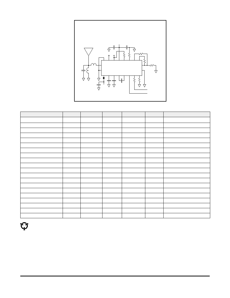
A S H T r a n s c e i v e r A p p l i c a t i o n C i r c u i t
A S K C o n f i g u r a t i o n
1
2 0
2
3
4
5
6
7
8
9
1 0
1 1
1 2
1 3
1 4
1 5
1 6
1 7
1 8
1 9
+ 3
V D C
R
P W
R
P R
R
T H 1
R
T H 2
R
R E F
R
L P F
R
T X M
C
B B O
C
P K D
C
A G C
C
R F B 2
C
D C B
L
A T
L
E S D
C
R F B 1
L
R F B
+
T / R / S
C
A T
Transceiver Set-Up, 3.0 Vdc, -40 to +85
0
C
CAUTION: Electrostatic Sensitive Device. Observe precautions when handling.

4
ASH Transceiver Theory of Operation
Introduction
RFM's amplifier-sequenced hybrid (ASH) transceiver is specifically
designed for short-range wireless data communication applications.
The transceiver provides robust operation, very small size, low
power consumption and low implementation cost. All critical RF
functions are contained in the hybrid, simplifying and speeding de-
sign-in. The ASH transceiver can be readily configured to support a
wide range of data rates and protocol requirements. The transceiver
features excellent suppression of transmitter harmonics and virtually
no RF emissions when receiving, making it easy to certify to short-
range (unlicensed) radio regulations.
Amplifier-Sequenced Receiver Operation
The ASH transceiver's unique feature set is made possible by its
system architecture. The heart of the transceiver is the amplifier-
sequenced receiver section, which provides more than 100 dB of
stable RF and detector gain without any special shielding or de-
coupling provisions. Stability is achieved by distributing the total RF
gain over time. This is in contrast to a superheterodyne receiver,
which achieves stability by distributing total RF gain over multiple
frequencies.
Figure 1 shows the basic block diagram and timing cycle for an am-
plifier-sequenced receiver. Note that the bias to RF amplifiers RFA1
and RFA2 are independently controlled by a pulse generator, and
that the two amplifiers are coupled by a surface acoustic wave
(SAW) delay line, which has a typical delay of 0.5 µs.
An incoming RF signal is first filtered by a narrow-band SAW filter,
and is then applied to RFA1. The pulse generator turns RFA1 ON
for 0.5 µs. The amplified signal from RFA1 emerges from the SAW
delay line at the input to RFA2. RFA1 is now switched OFF and
RFA2 is switched ON for 0.55 µs, amplifying the RF signal further.
The ON time for RFA2 is usually set at 1.1 times the ON time for
RFA1, as the filtering effect of the SAW delay line stretches the sig-
nal pulse from RFA1 somewhat. As shown in the timing diagram,
RFA1 and RFA2 are never on at the same time, assuring excellent
receiver stability. Note that the narrow-band SAW filter eliminates
sampling sideband responses outside of the receiver passband, and
the SAW filter and delay line act together to provide very high re-
ceiver ultimate rejection.
Amplifier-sequenced receiver operation has several interesting char-
acteristics that can be exploited in system design. The RF amplifiers
in an amplifier-sequenced receiver can be turned on and off almost
instantly, allowing for very quick power-down (sleep) and wake-up
times. Also, both RF amplifiers can be off between ON sequences
to trade-off receiver noise figure for lower average current consump-
tion. The effect on noise figure can be modeled as if RFA1 is on
continuously, with an attenuator placed in front of it with a loss
equivalent to 10*log
10
(RFA1 duty factor), where the duty factor is the
average amount of time RFA1 is ON (up to 50%). Since an
amplifier-sequenced receiver is inherently a sampling receiver, the
overall cycle time between the start of one RFA1 ON sequence and
A S H R e c e i v e r B l o c k D i a g r a m & T i m i n g C y c l e
A n t e n n a
P u l s e
G e n e r a t o r
S A W
D e l a y L i n e
S A W F i l t e r
R F A 1
R F A 2
D a t a
O u t
D e t e c t o r &
L o w - P a s s
F i l t e r
R F D a t a P u l s e
P 1
P 2
R F A 1 O u t
R F I n p u t
P 1
D e l a y L i n e
O u t
P 2
t
P W 2
t
P W 1
t
P R I
t
P R C
Figure 1

5
the start of the next RFA1 ON sequence should be set to sample
the narrowest RF data pulse at least 10 times. Otherwise, significant
edge jitter will be added to the detected data pulse.
ASH Transceiver Block Diagram
Figure 2 is the general block diagram of the ASH transceiver.
Please refer to Figure 2 for the following discussions.
Antenna Port
The only external RF components needed for the transceiver are
the antenna and its matching components. Antennas presenting an
impedance in the range of 35 to 72 ohms resistive can be satisfacto-
rily matched to the RFIO pin with a series matching coil and a shunt
matching/ESD protection coil. Other antenna impedances can be
matched using two or three components. For some impedances,
two inductors and a capacitor will be required. A DC path from RFIO
to ground is required for ESD protection.
Receiver Chain
The output of the SAW filter drives amplifier RFA1. This amplifier in-
cludes provisions for detecting the onset of saturation (AGC Set),
and for switching between 35 dB of gain and 5 dB of gain (Gain Se-
lect). AGC Set is an input to the AGC Control function, and Gain Se-
lect is the AGC Control function output. ON/OFF control to RFA1
(and RFA2) is generated by the Pulse Generator & RF Amp Bias
function. The output of RFA1 drives the SAW delay line, which has
a nominal delay of 0.5 µs.
The second amplifier, RFA2, provides 51 dB of gain below satura-
tion. The output of RFA2 drives a full-wave detector with 19 dB of
threshold gain. The onset of saturation in each section of RFA2 is
detected and summed to provide a logarithmic response. This is
added to the output of the full-wave detector to produce an overall
detector response that is square law for low signal levels, and tran-
sitions into a log response for high signal levels. This combination
provides excellent threshold sensitivity and more than 70 dB of
detector dynamic range. In combination with the 30 dB of AGC
range in RFA1, more than 100 dB of receiver dynamic range is
achieved.
The detector output drives a gyrator filter. The filter provides a
three-pole, 0.05 degree equiripple low-pass response with excellent
group delay flatness and minimal pulse ringing. The 3 dB bandwidth
of the filter can be set from 4.5 kHz to 1.8 MHz with an external re-
sistor.
The filter is followed by a base-band amplifier which boosts the de-
tected signal to the BBOUT pin. When the receiver RF amplifiers
are operating at a 50%-50% duty cycle, the BBOUT signal changes
about 10 mV/dB, with a peak-to-peak signal level of up to 685 mV.
For lower duty cycles, the mV/dB slope and peak-to-peak signal
level are proportionately less. The detected signal is riding on a
1.1 Vdc level that varies somewhat with supply voltage, tempera-
ture, etc. BBOUT is coupled to the CMPIN pin or to an external data
recovery process (DSP, etc.) by a series capacitor. The correct
value of the series capacitor depends on data rate, data run length,
and other factors as discussed in the ASH Transceiver Designer's
Guide.
When an external data recovery process is used with AGC, BBOUT
must be coupled to the external data recovery process and CMPIN
by separate series coupling capacitors. The AGC reset function is
driven by the signal applied to CMPIN.
When the transceiver is placed in power-down (sleep) or in a trans-
mit mode, the output impedance of BBOUT becomes very high. This
feature helps preserve the charge on the coupling capacitor to mini-
mize data slicer stabilization time when the transceiver switches
back to the receive mode.
Data Slicers
The CMPIN pin drives two data slicers, which convert the analog
signal from BBOUT back into a digital stream. The best data slicer
choice depends on the system operating parameters. Data slicer
DS1 is a capacitively-coupled comparator with provisions for an ad-
justable threshold. DS1 provides the best performance at low
A S H T r a n s c e i v e r B l o c k D i a g r a m
R F A 1
R F A 2
T X A 1
T X A 2
S A W
D e l a y L i n e
S A W
C R F i l t e r
L o g
A n t e n n a
R F I O
T u n i n g / E S D
D e t e c t o r
L o w - P a s s
F i l t e r
B B
A G C
C o n t r o l
P e a k
D e t e c t o r
P u l s e G e n e r a t o r
& R F A m p B i a s
L P F A D J
P R A T E
P W I D T H
R X D A T A
T X M O D
C N
T R L 1
C N
T R L 0
A G C C A P
R
R E F
T H L D 2
T H L D 1
M o d u l a t i o n
& B i a s C o n t r o l
P o w e r D o w n
C o n t r o l
G a i n S e l e c t
A G C S e t
A G C R e s e t
T h r e s h o l d
C o n t r o l
B B O U T
D S 2
D S 1
A N D
d B B e l o w
P e a k T h l d
R e f
T h l d
P K D E T
R e f
A G C
C
B B O
C
P K D
R
L P F
C
A G C
R
P R
R
P W
R
T H 2
R
T H 1
R
T X M
2 0
8
1 7
1 8
1 4
1 5
3
9
5
6
4
7
1 3
1 1
1 2
V C C 1 : P i n 2
V C C 2 : P i n 1 6
G N D 1 : P i n 1
G N D 2 : P i n 1 0
G N D 3 : P i n 1 9
R R E F : P i n 1 1
C M P I N : P i n 6
T X
I N
T u n i n g
Figure 2

signal-to-noise conditions. The threshold, or squelch, offsets the
comparator's slicing level from 0 to 90 mV, and is set with a resistor
between the RREF and THLD1 pins. This threshold allows a trade-
off between receiver sensitivity and output noise density in the
no-signal condition. For best sensitivity, the threshold is set to 0. In
this case, noise is output continuously when no signal is present.
This, in turn, requires the circuit being driven by the RXDATA pin to
be able to process noise (and signals) continuously.
This can be a problem if RXDATA is driving a circuit that must
"sleep" when data is not present to conserve power, or when it its
necessary to minimize false interrupts to a multitasking processor.
In this case, noise can be greatly reduced by increasing the thresh-
old level, but at the expense of sensitivity. The best 3 dB bandwidth
for the low-pass filter is also affected by the threshold level setting of
DS1. The bandwidth must be increased as the threshold is in-
creased to minimize data pulse-width variations with signal ampli-
tude.
Data slicer DS2 can overcome this compromise once the signal
level is high enough to enable its operation. DS2 is a "dB-below-
peak" slicer. The peak detector charges rapidly to the peak value of
each data pulse, and decays slowly in between data pulses (1:1000
ratio). The slicer trip point can be set from 0 to 120 mV below this
peak value with a resistor between RREF and THLD2. A threshold
of 60 mV is the most common setting, which equates to "6 dB below
peak" when RFA1 and RFA2 are running a 50%-50% duty cycle.
Slicing at the "6 dB-below-peak" point reduces the signal amplitude
to data pulse-width variation, allowing a lower 3 dB filter bandwidth
to be used for improved sensitivity.
DS2 is best for ASK modulation where the transmitted waveform
has been shaped to minimize signal bandwidth (TR3100). However,
DS2 is subject to being temporarily "blinded" by strong noise pulses,
which can cause burst data errors. Note that DS1 is active when
DS2 is used, as RXDATA is the logical AND of the DS1 and DS2
outputs. DS2 can be disabled by leaving THLD2 disconnected. A
non-zero DS1 threshold is required for proper AGC operation.
AGC Control
The output of the Peak Detector also provides an AGC Reset signal
to the AGC Control function through the AGC comparator. The pur-
pose of the AGC function is to extend the dynamic range of the re-
ceiver, so that two transceivers can operate close together when
running ASK and/or high data rate modulation. The onset of satura-
tion in the output stage of RFA1 is detected and generates the AGC
Set signal to the AGC Control function. The AGC Control function
then selects the 5 dB gain mode for RFA1. The AGC Comparator
will send a reset signal when the Peak Detector output (multiplied by
0.8) falls below the threshold voltage for DS1.
A capacitor at the AGCCAP pin avoids AGC "chattering" during the
time it takes for the signal to propagate through the low-pass filter
and charge the peak detector. The AGC capacitor also allows the
hold-in time to be set longer than the peak detector decay time to
avoid AGC chattering during runs of "0" bits in the received data
stream. Note that AGC operation requires the peak detector to be
functioning, even if DS2 is not being used. AGC operation can be
defeated by connecting the AGCCAP pin to Vcc. The AGC can be
latched ON once engaged by connecting a 150 kilohm resistor be-
tween the AGCCAP pin and ground in lieu of a capacitor.
Receiver Pulse Generator and RF Amplifier Bias
The receiver amplifier-sequence operation is controlled by the Pulse
Generator & RF Amplifier Bias module, which in turn is controlled by
the PRATE and PWIDTH input pins, and the Power Down (sleep)
Control Signal from the Modulation & Bias Control function.
In the low data rate mode, the interval between the falling edge of
one RFA1 ON pulse to the rising edge of the next RFA1 ON pulse
t
PRI
is set by a resistor between the PRATE pin and ground. The in-
terval can be adjusted between 0.1 and 5 µs. In the high data rate
mode (selected at the PWIDTH pin) the receiver RF amplifiers oper-
ate at a nominal 50%-50% duty cycle. In this case, the start-to-start
period t
PRC
for ON pulses to RFA1 are controlled by the PRATE re-
sistor over a range of 0.1 to 1.1 µs.
In the low data rate mode, the PWIDTH pin sets the width of the ON
pulse t
PW1
to RFA1 with a resistor to ground (the ON pulse width
t
PW2
to RFA2 is set at 1.1 times the pulse width to RFA1 in the low
data rate mode). The ON pulse width t
PW1
can be adjusted between
0.55 and 1 µs. However, when the PWIDTH pin is connected to Vcc
through a 1 M resistor, the RF amplifiers operate at a nominal
50%-50% duty cycle, facilitating high data rate operation (TR3100).
In this case, the RF amplifiers are controlled by the PRATE resistor
as described above.
Both receiver RF amplifiers are turned off by the Power Down Con-
trol Signal, which is invoked in the sleep and transmit modes.
Transmitter Chain
The transmitter chain consists of a SAW delay line oscillator fol-
lowed by a modulated buffer amplifier. The SAW filter suppresses
transmitter harmonics to the antenna. Note that the same SAW de-
vices used in the amplifier-sequenced receiver are reused in the
transmit modes.
Transmitter operation supports two modulation formats, on-off
keyed (OOK) modulation, and amplitude-shift keyed (ASK) modula-
tion which is normally used by the TR3100. When OOK modulation
is chosen, the transmitter output turns completely off between "1"
data pulses. When ASK modulation is chosen, a "1" pulse is repre-
sented by a higher transmitted power level, and a "0" is represented
by a lower transmitted power level. OOK modulation provides com-
patibility with first-generation ASH technology, and provides for
power conservation. ASK modulation must be used for high data
rates (data pulses less than 30 µs). ASK modulation also reduces
the effects of some types of interference and allows the transmitted
pulses to be shaped to control modulation bandwidth.
The modulation format is chosen by the state of the CNTRL0 and
the CNTRL1 mode control pins, as discussed below. When either
modulation format is chosen, the receiver RF amplifiers are turned
off. In the OOK mode, the delay line oscillator amplifier TXA1 and
buffer amplifier TXA2 are turned off when the voltage to the TXMOD
input falls below 220 mV. In the OOK mode, the data rate is limited
by the turn-on and turn-off times of the delay line oscillator, which
are 12 and 6 µs respectively. In the ASK mode TXA1 is biased ON
continuously, and the output of TXA2 is modulated by the TXMOD
input current. Minimum output power occurs in the ASK mode when
the modulation driver sinks about 10 µA of current from the TXMOD
pin.
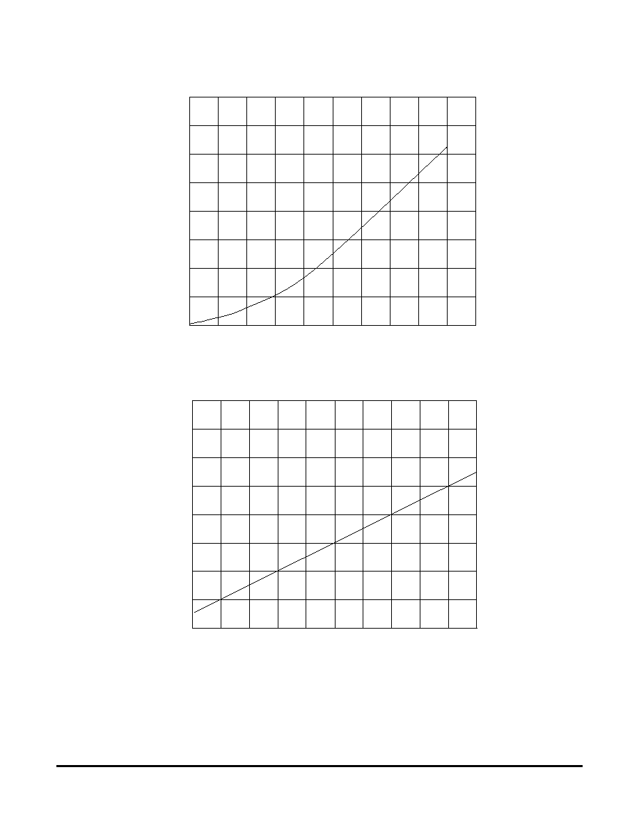
The transmitter RF output power is proportional to the input current
to the TXMOD pin. A series resistor is used to adjust the peak trans-
mitter output power. 0 dBm of output power requires about 250 µA
of input current.
Transceiver Mode Control
The four transceiver operating modes ≠ receive, transmit ASK,
transmit OOK, and power-down (sleep), are controlled by the Modu-
lation & Bias Control function, and are selected with the CNTRL1
6

and CNTRL0 control pins. Setting CNTRL1 and CNTRL0 both high
place the unit in the receive mode. Setting CNTRL1 high and
CNTRL0 low place the unit in the ASK transmit mode (TR1100).
Setting CNTRL1 low and CNTRL0 high place the unit in the OOK
transmit mode. Setting CNTRL1 and CNTRL0 both low place the
unit in the power-down (sleep) mode. Note that the resistor driving
TXMOD must be low in the receive and power-down modes. The
PWIDTH resistor must also be low in the power down mode to mini-
mize current. CNTRL1 and CNTRL0 are CMOS compatible inputs.
These inputs must be held at a logic level; they cannot be left un-
connected.
Transceiver Event Timing
Transceiver event timing is summarized in Table 1. Please refer to
this table for the following discussions.
Turn-On Timing
The maximum time t
PR
required for the receive function to become
operational at turn on is influenced by two factors. All receiver cir-
cuitry will be operational 5 ms after the supply voltage reaches
2.2 Vdc. The BBOUT-CMPIN coupling-capacitor is then DC stabi-
lized in 3 time constants (3*t
BBC
). The total turn-on time to stable re-
ceiver operation for a 10 ms power supply rise time is:
t
PR
= 15 ms + 3*t
BBC
The maximum time required for either the OOK or ASK transmitter
mode to become operational is 5 ms after the supply voltage
reaches 2.2 Vdc.
Receive-to-Transmit Timing
After turn on, the maximum time required to switch from receive to
either transmit mode is 12 µs. Most of this time is due to the start-up
of the transmitter oscillator.
Transmit-to-Receive Timing
The maximum time required to switch from the OOK or ASK trans-
mit mode to the receive mode is 3*t
BBC
, where t
BBC
is the BBOUT-
CMPIN coupling-capacitor time constant. When the operating tem-
perature is limited to 60
o
C, the time required to switch from transmit
to receive is dramatically less for short transmissions, as less
charge leaks away from the BBOUT-CMPIN coupling capacitor.
Sleep and Wake-Up Timing
The maximum transition time from the receive mode to the
power-down (sleep) mode t
RS
is 10 µs after CNTRL1 and CNTRL0
are both low (1 µs fall time).
The maximum transition time from either transmit mode to the sleep
mode (t
TOS
and t
TAS
) is 10 µs after CNTRL1 and CNTRL0 are both
low (1 µs fall time).
The maximum transition time t
SR
from the sleep mode to the receive
mode is 3*t
BBC
, where t
BBC
is the BBOUT-CMPIN coupling-capacitor
time constant. When the operating temperature is limited to 60
o
C,
the time required to switch from sleep to receive is dramatically less
for short sleep times, as less charge leaks away from the BBOUT-
CMPIN coupling capacitor.
The maximum time required to switch from the sleep mode to either
transmit mode (t
STO
and t
STA
) is 16 µs. Most of this time is due to the
start-up of the transmitter oscillator.
AGC Timing
The maximum AGC engage time t
AGC
is 5 µs after the reception of a
-30 dBm RF signal with a 1 µs envelope rise time.
The minimum AGC hold-in time is set by the value of the capacitor
at the AGCCAP pin. The hold-in time t
AGH
= C
AGC
/19.1, where t
AGH
is
in µs and C
AGC
is in pF.
Peak Detector Timing
The Peak Detector attack time constant is set by the value of the ca-
pacitor at the PKDET pin. The attack time t
PKA
= C
PKD
/4167, where
t
PKA
is in µs and C
PKD
is in pF. The Peak Detector decay time con-
stant t
PKD
= 1000*t
PKA
.
Pulse Generator Timing
In the low data rate mode, the interval t
PRI
between the falling edge
of an ON pulse to the first RF amplifier and the rising edge of the
next ON pulse to the first RF amplifier is set by a resistor R
PR
be-
tween the PRATE pin and ground. The interval can be adjusted be-
tween 0.1 and 5 µs with a resistor in the range of 51 K to 2000 K.
The value of the R
PR
is given by:
R
PR
= 404* t
PRI
+ 10.5, where t
PRI
is in µs, and R
PR
is in kilohms
In the high data rate mode normally use by the TR3100 (selected at
the PWIDTH pin), the receiver RF amplifiers operate at a nominal
50%-50% duty cycle. In this case, the period t
PRC
from the start of
an ON pulse to the first RF amplifier to the start of the next ON
pulse to the first RF amplifier is controlled by the PRATE resistor
over a range of 0.1 to 1.1 µs using a resistor of 11 K to 220 K. In
this case R
PR
is given by:
R
PR
= 198* t
PRC
- 8.51, where t
PRC
is in µs and R
PR
is in kilohms
In the low data rate mode, the PWIDTH pin sets the width of the ON
pulse to the first RF amplifier t
PW1
with a resistor R
PW
to ground (the
ON pulse width to the second RF amplifier t
PW2
is set at 1.1 times
the pulse width to the first RF amplifier in the low data rate mode).
The ON pulse width t
PW1
can be adjusted between 0.55 and 1 µs
with a resistor value in the range of 200 K to 390 K. The value of
R
PW
is given by:
R
PW
= 404* t
PW1
- 18.6, where t
PW1
is in µs and R
PW
is in kilohms
However, when the PWIDTH pin is connected to Vcc through a 1 M
resistor, the RF amplifiers operate at a nominal 50%-50% duty cy-
cle, facilitating high data rate operation. In this case, the RF amplifi-
ers are controlled by the PRATE resistor as described above.
LPF Group Delay
The low-pass filter group delay is a function of the filter 3 dB band-
width, which is set by a resistor R
LPF
to ground at the LPFADJ pin.
The minimum 3 dB bandwidth f
LPF
= 1445/R
LPF
, where f
LPF
is in kHz,
and R
LPF
is in kilohms.
The maximum group delay t
FGD
= 1750/f
LPF
= 1.21*R
LPF
, where t
FGD
is in µs, f
LPF
in kHz, and R
LPF
in kilohms.
7
Event
Symbol
Time
Min/Max
Test
Conditions
Notes
Turn
On
to
Receive
t
PR
3*t
BBC
+
1
5
m
s
max
10
ms
supply
voltage
rise
time
time
until
receiver
operational
Turn
On
to
TXOOK
t
PTO
15
ms
max
10
ms
supply
voltage
rise
time
time
until
TXMOD
can
modulate
transmitter
Turn
On
to
TXASK
t
PTA
15
ms
max
10
ms
supply
voltage
rise
time
time
until
TXMOD
can
modulate
transmitter
RX
to
TXOOK
t
RTO
12
µs
max
1
µ
s
CNTRL1
fall
time
TXMOD
low
1
µ
s
before
CNTRL1
falls
RX
to
TXASK
t
RTA
12
µs
max
1
µ
s
CNTRL0
fall
time
TXMOD
low
1
µ
s
before
CNTRL0
falls
TXOOK
to
RX
t
TOR
3*t
BBC
max
1
µ
s
CNTRL1
rise
time
time
until
receiver
operational
TXASK
to
RX
t
TAR
3*t
BBC
max
1
µ
s
CNTRL0
rise
time
time
until
receiver
operational
Sleep
to
RX
t
SR
3*t
BBC
max
1µs
CNTRL0/CNTROL1
rise
times
time
until
receiver
operational
Sleep
to
TXOOK
t
STO
16
µs
max
1
µ
s
CNTRL0
rise
time
time
until
TXMOD
can
modulate
transmitter
Sleep
to
TXASK
t
STA
16
µs
max
1
µ
s
CNTRL1
rise
time
time
until
TXMOD
can
modulate
transmitter
RX
to
Sleep
t
RS
10
µs
max
1µs
CNTRL0/CNTROL1
fall
times
time
until
transceiver
is
in
power-down
mode
TXOOK
to
Sleep
t
TOS
10
µs
max
1
µ
s
CNTRL0
fall
time
time
until
transceiver
is
in
power-down
mode
TXASK
to
Sleep
t
TAS
10
µs
max
1
µ
s
CNTRL1
fall
time
time
until
transceiver
is
in
power-down
mode
AGC
Engage
t
AGC
5
µ
s
max
1
µ
s
rise
time,
-30
dBm
signal
RFA1
switches
from
35
to
5
d
B
gain
AGC
Hold-In
t
AGH
C
AGC/
19.1
min
CAGC
in
pF,
t
AGH
in
µs
user
selected;
longer
than
t
PKD
PKDET
Attack
Time
Constant
t
PKA
C
PKD
/4167
min
C
PKD
in
pF,
t
PKA
in
µs
user
selected
PKDET
Decay
Time
Constant
t
PKD
1000*t
PKA
min
t
PKD
and
t
PKA
in
µs
slaved
to
attack
time
PRATE
Interval
t
PRI
0.1
to
5
µ
s
range
low
data
rate
mode
user
selected
mode
PWIDTH
RFA1
t
PW1
0.55
to
1
µ
s
range
low
data
rate
mode
user
selected
mode
PWIDTH
RFA2
t
PW2
1.1*t
PW1
range
low
data
rate
mode
user
selected
mode
PRATE
Cycle
t
PRC
0.1
to
1.1
µs
range
high
data
rate
mode
user
selected
mode
PWIDTH
High
(RFA1
&
RFA2)
t
PWH
0.05
to
0.55
µs
range
high
data
rate
mode
user
selected
mode
LPF
Group
Delay
t
FGD
1750/f
LPF
max
t
FGD
in
µs,
f
LPF
in
kHz
user
selected
LPF
3
d
B
Bandwidth
f
LPF
1445/R
LPF
min
f
LPF
in
kHz,
R
LPF
in
kilohms
user
selected
BBOUT-CMPIN
Time
Constant
t
BBC
0.064*C
BBO
min
t
BBC
in
µs,
C
BBO
in
pF
user
selected
Transceiver
Event
Timing,
3.0
Vdc,
-40
to
+85
0
C
Table
1

Pin
Name
Description
1
GND1
GND1 is the RF ground pin. GND2 and GND3 should be connected to GND1 by short, low-inductance traces.
2
VCC1
VCC1 is the positive supply voltage pin for the transmitter output amplifier and the receiver base-band circuitry.
VCC1 is usually connected to the positive supply through a ferrite RF decoupling bead, which is bypassed by an
RF capacitor on the supply side. See the ASH Transceiver Designer's Guide for additional information.
3
AGCCAP
This pin controls the AGC reset operation. A capacitor between this pin and ground sets the minimum time the
AGC will hold-in once it is engaged. The hold-in time is set to avoid AGC chattering. For a given hold-in time t
AGH
,
the capacitor value C
AGC
is:
C
AGC
= 19.1* t
AGH
, where t
AGH
is in µs and C
AGC
is in pF
A ±10% ceramic capacitor should be used at this pin. The value of C
AGC
given above provides a hold-in time be-
tween t
AGH
and 2.65* t
AGH
, depending on operating voltage, temperature, etc. The hold-in time is chosen to allow
the AGC to ride through the longest run of zero bits that can occur in a received data stream. The AGC hold-in
time can be greater than the peak detector decay time, as discussed below. However, the AGC hold-in time
should not be set too long, or the receiver will be slow in returning to full sensitivity once the AGC is engaged by
noise or interference. The use of AGC is optional when using OOK modulation with data pulses of at least 30 µs.
AGC operation can be defeated by connecting this pin to Vcc. Active or latched AGC operation is required for
ASK modulation and/or for data pulses of less than 30 µs. The AGC can be latched on once engaged by connect-
ing a 150 K resistor between this pin and ground, instead of a capacitor. AGC operation depends on a functioning
peak detector, as discussed below. The AGC capacitor is discharged in the receiver power-down (sleep) mode
and in the transmit modes.
4
PKDET
This pin controls the peak detector operation. A capacitor between this pin and ground sets the peak detector at-
tack and decay times, which have a fixed 1:1000 ratio. For most applications, these time constants should be co-
ordinated with the base-band time constant. For a given base-band capacitor C
BBO
, the capacitor value C
PKD
is:
C
PKD
= 0.33* C
BBO
, where C
BBO
and C
PKD
are in pF
A ±10% ceramic capacitor should be used at this pin. This time constant will vary between t
PKA
and 1.5* t
PKA
with
variations in supply voltage, temperature, etc. The capacitor is driven from a 200 ohm "attack" source, and decays
through a 200 K load. The peak detector is used to drive the "dB-below-peak" data slicer and the AGC release
function. The AGC hold-in time can be extended beyond the peak detector decay time with the AGC capacitor, as
discussed above. Where low data rates and OOK modulation are used, the "dB-below-peak" data slicer and the
AGC are optional. In this case, the PKDET pin and the THLD2 pin can be left unconnected, and the AGC pin can
be connected to Vcc to reduce the number of external components needed. The peak detector capacitor is dis-
charged in the receiver power-down (sleep) mode and in the transmit modes.
5
BBOUT
BBOUT is the receiver base-band output pin. This pin drives the CMPIN pin through a coupling capacitor C
BBO
for
internal data slicer operation. The time constant t
BBC
for this connection is:
t
BBC
= 0.064*C
BBO
, where t
BBC
is in µs and C
BBO
is in pF
A ±10% ceramic capacitor should be used between BBOUT and CMPIN. The time constant can vary between t
BBC
and 1.8*t
BBC
with variations in supply voltage, temperature, etc. The optimum time constant in a given circum-
stance will depend on the data rate, data run length, and other factors as discussed in the ASH Transceiver De-
signer's Guide. A common criteria is to set the time constant for no more than a 20% voltage droop during SP
MAX
.
For this case:
C
BBO
= 70*SP
MAX
, where SP
MAX
is the maximum signal pulse width in µs and C
BBO
is in pF
The output from this pin can also be used to drive an external data recovery process (DSP, etc.). The nominal out-
put impedance of this pin is 1 K. When the receiver RF amplifiers are operating at a 50%-50% duty cycle, the
BBOUT signal changes about 10 mV/dB, with a peak-to-peak signal level of up to 685 mV. For lower duty cycles,
the mV/dB slope and peak-to-peak signal level are proportionately less. The signal at BBOUT is riding on a
1.1 Vdc value that varies somewhat with supply voltage and temperature, so it should be coupled through a ca-
pacitor to an external load. A load impedance of 50 K to 500 K in parallel with no more than 10 pF is recom-
mended. When an external data recovery process is used with AGC, BBOUT must be coupled to the external
data recovery process and CMPIN by separate series coupling capacitors. The AGC reset function is driven by
the signal applied to CMPIN. When the transceiver is in power-down (sleep) or in a transmit mode, the output im-
pedance of this pin becomes very high, preserving the charge on the coupling capacitor.
6
CMPIN
This pin is the input to the internal data slicers. It is driven from BBOUT through a coupling capacitor. The input
impedance of this pin is 70 K to 100 K.
7
RXDATA
RXDATA is the receiver data output pin. This pin will drive a 10 pF, 500 K parallel load. The peak current available
from this pin increases with the receiver low-pass filter cutoff frequency. In the power-down (sleep) or transmit
modes, this pin becomes high impedance. If required, a 1000 K pull-up or pull-down resistor can be used to estab-
lish a definite logic state when this pin is high impedance. If a pull-up resistor is used, the positive supply end
should be connected to a voltage no greater than Vcc + 200 mV.
9
Pin Descriptions

Pin
Name
Description
8
TXMOD
The transmitter RFoutput voltage is proportional to the input current to this pin. A series resistor is used to adjust
the peak transmitter output voltage. 0 dBm of output power requires about 250 µA of input current. In the ASK
mode, minimum output power occurs when the modulation driver sinks about 10 µA of current from this pin. In the
OOK mode, input signals less than 220 mV completely turn the transmitter oscillator off. Internally, this pin ap-
pears to be a diode in series with a small resistor. Peak transmitter output power P
O
for a 3 Vdc supply voltage is
approximately:
P
O
= 16*(I
TXM
)
2
, where P
O
is in mW, and the peak modulation current I
TXM
is in mA
A ±5% resistor value is recommended. In the ASK mode (TR3100), this pin accepts analog modulation (shaped or
unshaped data pulses). ASK modulation is practical for data pulses 1 µs or longer. The resistor driving this pin
must be low in the receive and power-down (sleep) modes. Please refer to the ASH Transceiver Designer's Guide
for additional information on modulation techniques.
9
LPFADJ
This pin is the receiver low-pass filter bandwidth adjust. The filter bandwidth is set by a resistor R
LPF
between this
pin and ground. The resistor value can range from 330 K to 820 ohms, providing a filter 3 dB bandwidth f
LPF
from
4.5 kHz to 1.8 MHz. The resistor value is determined by:
R
LPF
= 1445/ f
LPF
, where R
LPF
is in kilohms, and f
LPF
is in kHz
A ±5% resistor should be used to set the filter bandwidth. This will provide a 3 dB filter bandwidth between f
LPF
and 1.3* f
LPF
with variations in supply voltage, temperature, etc. The filter provides a three-pole, 0.05 degree
equiripple phase response. The peak drive current available from RXDATA increases in proportion to the filter
bandwidth setting.
10
GND2
GND2 is an IC ground pin. It should be connected to GND1 by a short, low inductance trace.
11
RREF
RREF is the external reference resistor pin. A 100 K reference resistor is connected between this pin and ground.
A ±1% resistor tolerance is recommended. It is important to keep the total capacitance between ground, Vcc and
this node to less than 5 pF to maintain current source stability. If THLD1 and/or THDL2 are connected to RREF
through resistor values less that 1.5 K, their node capacitance must be added to the RREF node capacitance and
the total should not exceed 5 pF.
12
THLD2
THLD2 is the "dB-below-peak" data slicer (DS2) threshold adjust pin. The threshold is set by a 0 to 200 K resistor
R
TH2
between this pin and RREF. Increasing the value of the resistor decreases the threshold below the peak de-
tector value (increases difference) from 0 to 120 mV. For most applications, this threshold should be set at 6 dB
below peak, or 60 mV for a 50%-50% RF amplifier duty cycle. The value of the THLD2 resistor is given by:
R
TH2
= 1.67*V, where R
TH2
is in kilohms and the threshold V is in mV
A ±1% resistor tolerance is recommended for the THLD2 resistor. Leaving the THLD2 pin open disables the
dB-below-peak data slicer operation.
13
THLD1
The THLD1 pin sets the threshold for the standard data slicer (DS1) through a resistor R
TH1
to RREF. The thresh-
old is increased by increasing the resistor value. Connecting this pin directly to RREF provides zero threshold.
The value of the resistor depends on whether THLD2 is used. For the case that THLD2 is not used, the accept-
able range for the resistor is 0 to 100 K, providing a THLD1 range of 0 to 90 mV. The resistor value is given by:
R
TH1
= 1.11*V, where R
TH1
is in kilohms and the threshold V is in mV
For the case that THLD2 is used, the acceptable range for the THLD1 resistor is 0 to 200 K, again providing a
THLD1 range of 0 to 90 mV. The resistor value is given by:
R
TH1
= 2.22*V, where R
TH1
is in kilohms and the threshold V is in mV
A ±1% resistor tolerance is recommended for the THLD1 resistor. Note that a non-zero DS1 threshold is required
for proper AGC operation.
14
PRATE
The interval between the falling edge of an ON pulse to the first RF amplifier and the rising edge of the next ON
pulse to the first RF amplifier t
PRI
is set by a resistor R
PR
between this pin and ground. The interval t
PRI
can be ad-
justed between 0.1 and 5 µs with a resistor in the range of 51 K to 2000 K. The value of R
PR
is given by:
R
PR
= 404* t
PRI
+ 10.5, where t
PRI
is in µs, and R
PR
is in kilohms
A ±5% resistor value is recommended. When the PWIDTH pin is connected to Vcc through a 1 M resistor, the RF
amplifiers operate at a nominal 50%-50% duty cycle, facilitating high data rate operation (TR3100). In this case,
the period t
PRC
from start-to-start of ON pulses to the first RF amplifier is controlled by the PRATE resistor over a
range of 0.1 to 1.1 µs using a resistor of 11 K to 220 K. In this case the value of R
PR
is given by:
R
PR
= 198* t
PRC
- 8.51, where t
PRC
is in µs and R
PR
is in kilohms
A ±5% resistor value should also be used in this case. Please refer to the ASH Transceiver Designer's Guide for
additional amplifier duty cycle information. It is important to keep the total capacitance between ground, Vcc and
this pin to less than 5 pF to maintain stability.
10

Pin
Name
Description
15
PWIDTH
The PWIDTH pin sets the width of the ON pulse to the first RF amplifier t
PW1
with a resistor R
PW
to ground (the ON
pulse width to the second RF amplifier t
PW2
is set at 1.1 times the pulse width to the first RF amplifier). The ON
pulse width t
PW1
can be adjusted between 0.55 and 1 µs with a resistor value in the range of 200 K to 390 K. The
value of R
PW
is given by:
R
PW
= 404* t
PW1
- 18.6, where t
PW1
is in µs and R
PW
is in kilohms
A ±5% resistor value is recommended. When this pin is connected to Vcc through a 1 M resistor, the RF amplifi-
ers operate at a nominal 50%-50% duty cycle, facilitating high data rate operation. In this case, the RF amplifier
ON times are controlled by the PRATE resistor as described above. It is important to keep the total capacitance
between ground, Vcc and this node to less than 5 pF to maintain stability. When using the high data rate operation
with the sleep mode, connect the 1 M resistor between this pin and CNTRL1 (Pin 17), so this pin is low in the
sleep mode.
16
VCC2
VCC2 is the positive supply voltage pin for the receiver RF section and transmitter oscillator. Pin 16 must be by-
passed with an RF capacitor, and must also be bypassed with a 1 to 10 µF tantalum or electrolytic capacitor. See
the ASH Transceiver Designer's Guide for additional information.
17
CNTRL1
CNTRL1 and CNTRL0 select the receive and transmit modes. CNTRL1 and CNTRL0 both high place the unit in
the receive mode. CNTRL1 high and CNTRL0 low place the unit in the ASK transmit mode (TR3100). CNTRL1
low and CNTRL0 high place the unit in the OOK transmit mode. CNTRL1 and CNTRL0 both low place the unit in
the power-down (sleep) mode. CNTRL1 is a high-impedance input (CMOS compatible). An input voltage of 0 to
300 mV is interpreted as a logic low. An input voltage of Vcc - 300 mV or greater is interpreted as a logic high. An
input voltage greater than Vcc + 200 mV should not be applied to this pin. A logic high requires a maximum
source current of 40 µA. A logic low requires a maximum sink current of 25 µA (1 µA in sleep mode). This pin
must be held at a logic level; it cannot be left unconnected.
18
CNTRL0
CNTRL0 is used with CNTRL1 to control the receive and transmit modes of the transceiver. CNTRL0 is a
high-impedance input (CMOS compatible). An input voltage of 0 to 300 mV is interpreted as a logic low. An input
voltage of Vcc - 300 mV or greater is interpreted as a logic high. An input voltage greater than Vcc + 200 mV
should not be applied to this pin. A logic high requires a maximum source current of 40 µA. A logic low requires a
maximum sink current of 25 µA (1 µA in sleep mode). This pin must be held at a logic level; it cannot be left un-
connected.
19
GND3
GND3 is an IC ground pin. It should be connected to GND1 by a short, low inductance trace.
20
RFIO
RFIO is the RF input/output pin. This pin is connected directly to the SAW filter transducer. Antennas presenting
an impedance in the range of 35 to 72 ohms resistive can be satisfactorily matched to this pin with a series match-
ing coil and a shunt matching/ESD protection coil. Other antenna impedances can be matched using two or three
components. For some impedances, two inductors and a capacitor will be required. A DC path from RFIO to
ground is required for ESD protection.
11
S M - 2 0 H P C B P a d L a y o u t
D i m e n s i o n s i n i n c h e s .
. 0 9
. 3 7 0
0 . 0 0 0
0.
000
. 0 6 5
. 1 0 5
. 1 4 5
. 1 8 5
. 2 2 5
. 2 6 5
. 3 0 5
. 3 4 5
.0
9
0
. 4 3 5
.1
2
2
5
.1
6
2
5
.1
4
7
5
.1
8
7
5
.2
2
0
.3
1
0
12
file: tr3100y.vp, 2003.07.17 rev
Note: Specifications subject to change without notice.
0 . 2 0
0 . 4 0
0 . 6 0
0 . 8 0
1 . 0 0
1 . 2 0
1 . 4 0
1 . 6 0
3 V
R F O u t p u t P o w e r v s I
T X M
I
T X M
i n µ A
O
u
t
p
u
t
P
ow
e
r
in
m
W
2 5
5 0
7 5
1 0 0
1 2 5
1 5 0
1 7 5
2 0 0
2 7 5
2 5 0
2 2 5
I
T X M
i n µ A
V
T X M
v s I
T X M
0 . 8 5
0 . 9 0
0 . 9 5
1 . 0 0
1 . 0 5
1 . 1 0
1 . 1 5
1 . 2 0
V
TX
M
in
V
2 5
5 0
7 5
1 0 0
1 2 5
1 5 0
1 7 5
2 0 0
2 7 5
2 5 0
2 2 5