11-43
11
T
RAN
SCE
I
V
E
RS
�
�
�
�
��
�
RF Micro Devices, Inc.
7625 Thorndike Road
Greensboro, NC 27409, USA
Tel (336) 664 1233
Fax (336) 664 0454
http://www.rfmd.com
��
Si BJT
GaAs MESFET
GaAs HBT
Si Bi-CMOS
SiGe HBT
Si CMOS
F
TX
/n
Rolling
Code
Encoder
S1
S4
S3
S2
Antenna
Ref
�
32 or
�
64
RF2516
PD
VCO
DK1001T
�
�
� Remote Keyless Entry
� Wireless Security Systems
� Remote Controls
� Remote Monitoring
The DK1001T is the transmitter half of our remote keyless
entry system evaluation kit. It is designed to allow the
user to easily and quickly demonstrate the operation of
the RF2516 in a typical application. Everything needed to
demonstrate a one way transmitter is included. The
RF2516 is setup to demonstrate a typical keyless entry
system using a rolling code encoder while operating at
433MHz. A battery is included and the antenna is printed
on the circuit board. This unit is designed to work with the
mating receiver, DK1001R.
� Complete Transmitter
� Programmable Rolling Code Encoder
� Four Pushbutton Functionality
� LED Indicator
� Mates With DK1001R Receiver
� Battery and Antenna
DK1001T
Available only as part of the DK1001 Reference
Design Kit
Rev A0 000330

11-44
DK1001T
Rev A0 000330
11
T
RAN
SCE
I
V
E
RS
Absolute Maximum Ratings
Parameter
Rating
Unit
Supply Voltage
-0.5 to +3.6
V
DC
Operating Ambient Temperature
-40 to +85
�C
Storage Temperature
-40 to +150
�C
Parameter
Specification
Unit
Condition
Min.
Typ.
Max.
Overall
T = 25�C, V
CC
=3.0V, Freq=433MHz
Frequency Range
433
MHz
Modulation
OOK
Modulation Frequency
1
kHz
Set by mode of encoder.
Output Power
70
dB
�
V/m
Measured in GTEM test cell
ON/OFF Ratio
75
dB
PLL and Prescaler
Prescaler Divide Ratio
32
PLL Phase Noise
-97
dBc/Hz
10kHz Offset, 50kHz loop bandwidth
-102
dBc/Hz
100kHz Offset, 50kHz loop bandwidth
Harmonics (average)
35
dB
�
V/m
Measured in GTEM test cell.
Reference Frequency
13.562
MHz
Crystal Frequency Spurs
25
dB
�
V/m
Measured in GTEM test cell.
Power Supply
Voltage
3.0
V
Specifications
2.0
3.0
V
Operating limits
Current Consumption (Avg.)
4
7
9
mA
Caution! ESD sensitive device.
RF Micro Devices believes the furnished information is correct and accurate
at the time of this printing. However, RF Micro Devices reserves the right to
make changes to its products without notice. RF Micro Devices does not
assume responsibility for the use of the described product(s).

11-45
DK1001T
Rev A0 000330
11
T
RAN
SCE
I
V
E
RS
�
Introduction
The small 3V lithium button cell is installed in the back
of the transmitter board by sliding the battery com-
pletely into the clip provided. The larger flat surface of
the battery, marked with a "+" should be in contact with
the clip, also marked with a "+" and should be facing
away from the printed circuit board. It will normally
require some force to insert the battery completely.
When the batteries are first installed and the devices
are activated, the receiver may not recognize the trans-
mitter. This is normal and only indicates that the
receiver must learn the transmitter. This is accom-
plished with the following procedure:
1. Install the batteries, if not already installed
2. Turn on the receiver using the power switch as
described above
3. Momentarily depress the button marked "LEARN"
on the receiver. This may be accessed through an
opening in the clear cover on the front of the
receiver with a small tool. This will cause the LED
located next to the button to be illuminated.
4. While the LED is illuminated, depress any button on
the transmitter. When a button on the transmitter is
depressed, the LED on the transmitter will be illumi-
nated. Continue depressing the button on the trans-
mitter until the LED on the receiver is no longer
illuminated. Release the button on the transmitter.
5. Depress a button on the transmitter once again.
Continue depressing the button until the LED on the
receiver begins to flash. Release the button on the
transmitter.
6. The LED on the receiver will stop flashing. The pro-
cess is complete.
7. To verify proper operation, depress any button on
the transmitter. An LED on the receiver should be
illuminated and the LED located next to the
"LEARN" button should flash. When one of the but-
tons on the transmitter is depressed, the buzzer will
sound.
The transmitter has four pushbuttons that activate the
transmitter. The four buttons represent four separate
functions that could be activated using the system.
This evaluation board uses the Microchip encoder chip
for secure transmissions. Further information about
this device may be obtained from Microchip Technol-
ogy Inc., Chandler, Arizona, USA. An LED is included
to indicate that the device is activated and four pads
are included for programming the HCS300 device. The
device is preprogrammed with a dummy serial number.
An antenna is printed onto the circuit board for conve-
nience. The transmitter is simply operated by pressing
any of the buttons. While the button is depressed, the
LED on the transmitter is illuminated.
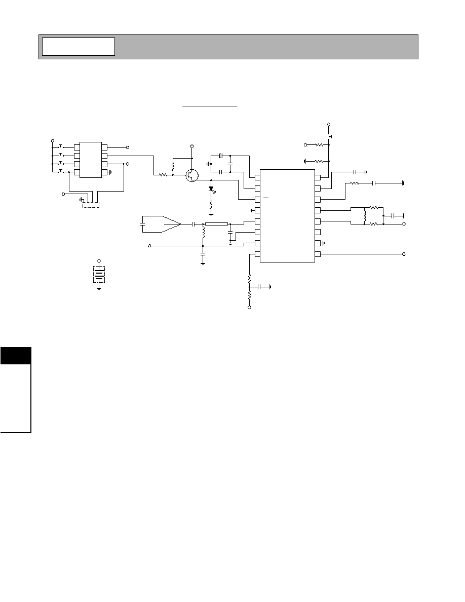
The 433MHz transmitter uses a 13.562MHz crystal
which may be identified by the label on the top of the
crystal can. The following pages show the schematic
for the 433 MHz transmitter, the bill of material for the
433MHz transmitter, the printed circuit board layout for
the 433MHz transmitter. These materials, along with
the Gerber files for the PCBs may be found on the
Internet at
www.rfmd.com
.