 | –≠–ª–µ–∫—Ç—Ä–æ–Ω–Ω—ã–π –∫–æ–º–ø–æ–Ω–µ–Ω—Ç: NBB-400 | –°–∫–∞—á–∞—Ç—å:  PDF PDF  ZIP ZIP |
4-33
Product Description
Ordering Information
Typical Applications
Features
Functional Block Diagram
RF Micro Devices, Inc.
7628 Thorndike Road
Greensboro, NC 27409, USA
Tel (336) 664 1233
Fax (336) 664 0454
http://www.rfmd.com
Optimum Technology MatchingÆ Applied
Si BJT
GaAs MESFET
GaAs HBT
Si Bi-CMOS
SiGe HBT
Si CMOS
InGaP/HBT
GaN HEMT
SiGe Bi-CMOS
1
3
2
4
RF OUT
RF IN
GND
GND
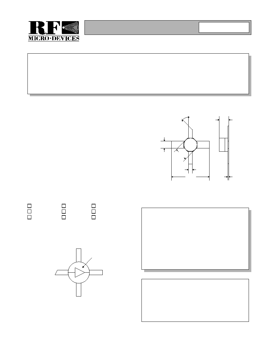
MARKING - N4
NBB-400
CASCADABLE BROADBAND
GaAs MMIC AMPLIFIER DC TO 8GHz
∑ Narrow and Broadband Commercial and
Military Radio Designs
∑ Linear and Saturated Amplifiers
∑ Gain Stage or Driver Amplifiers for
MWRadio/Optical Designs (PTP/PMP/
LMDS/UNII/VSAT/WLAN/Cellular/DWDM)
The NBB-400 cascadable broadband InGaP/GaAs MMIC
amplifier is a low-cost, high-performance solution for gen-
eral purpose RF and microwave amplification needs. This
50
gain block is based on a reliable HBT proprietary
MMIC design, providing unsurpassed performance for
small-signal applications. Designed with an external bias
resistor, the NBB-400 provides flexibility and stability. The
NBB-400 is packaged in a low-cost, surface-mount
ceramic package, providing ease of assembly for high-
volume tape-and-reel requirements. It is available in
either packaged or chip (NBB-400-D) form, where its gold
metallization is ideal for hybrid circuit designs.
∑ Reliable, Low-Cost HBT Design
∑ 15.5dB Gain, +15.0dBm P1dB@2GHz
∑ High P1dB of +14.6dBm@6.0GHz
∑ Single Power Supply Operation
∑ 50
I/O Matched for High Freq. Use
NBB-400
Cascadable Broadband GaAs MMIC Amplifier DC to
8GHz
NBB-400-T1 or -T3Tape & Reel, 1000 or 3000 Pieces (respectively)
NBB-400-D
NBB-400 Chip Form (100 pieces minimum order)
NBB-400-E
Fully Assembled Evaluation Board
NBB-X-K1
Extended Frequency InGaP Amp Designer's Tool Kit
0
Rev A4 030912
UNITS:
Inches
(mm)
N4
0.070
(1.78)
0.040
(1.02)
0.020
0.200 sq.
(5.08)
45∞
0.055
(1.40)
0.005
(0.13)
Package Style: Micro-X, 4-Pin, Ceramic

4-34
NBB-400
Rev A4 030912
Absolute Maximum Ratings
Parameter
Rating
Unit
RF Input Power
+20
dBm
Power Dissipation
300
mW
Device Current
70
mA
Channel Temperature
200
∞C
Operating Temperature
-45 to +85
∞C
Storage Temperature
-65 to +150
∞C
Exceeding any one or a combination of these limits may cause permanent damage.
Parameter
Specification
Unit
Condition
Min.
Typ.
Max.
Overall
V
D
=+3.9V, I
CC
=47mA, Z
0
=50
, T
A
=+25∞C
Small Signal Power Gain, S21
15.5
16.7
dB
f=0.1GHz to 1.0GHz
16.5
dB
f=1.0GHz to 4.0GHz
16.0
dB
f=4.0GHz to 6.0GHz
12.5
13.5
dB
f=6.0GHz to 8.0GHz
Gain Flatness, GF
±0.8
dB
f=0.1GHz to 5.0GHz
Input and Output VSWR
1.45:1
f=0.1GHz to 4.0GHz
1.30:1
f=4.0GHz to 6.0GHz
1.90:1
f=6.0GHz to 12.0GHz
Bandwidth, BW
7.5
GHz
BW3 (3dB)
Output Power @
-1dB Compression, P1dB
13.0
dBm
f=2.0GHz
14.6
dBm
f=6.0GHz
13.5
dBm
f=9.0GHz
Noise Figure, NF
4.3
dB
f=3.0GHz
Third Order Intercept, IP3
+28.1
dBm
f=2.0GHz
Reverse Isolation, S12
-17.5
dB
f=0.1GHz to 12.0GHz
Device Voltage, V
D
3.6
3.9
4.2
V
Gain Temperature Coefficient,
G
T
/
T
-0.0015
dB/∞C
MTTF versus Temperature
@ I
CC
=50mA
Case Temperature
85
∞C
Junction Temperature
131
∞C
MTTF
>1,000,000
hours
Thermal Resistance
JC
251
∞C/W
J
T
T
CASE
≠
V
D
I
CC
---------------------------
JC
∞C Watt
/
(
)
=
Caution! ESD sensitive device.
RF Micro Devices believes the furnished information is correct and accurate
at the time of this printing. However, RF Micro Devices reserves the right to
make changes to its products without notice. RF Micro Devices does not
assume responsibility for the use of the described product(s).
4-35
NBB-400
Rev A4 030912
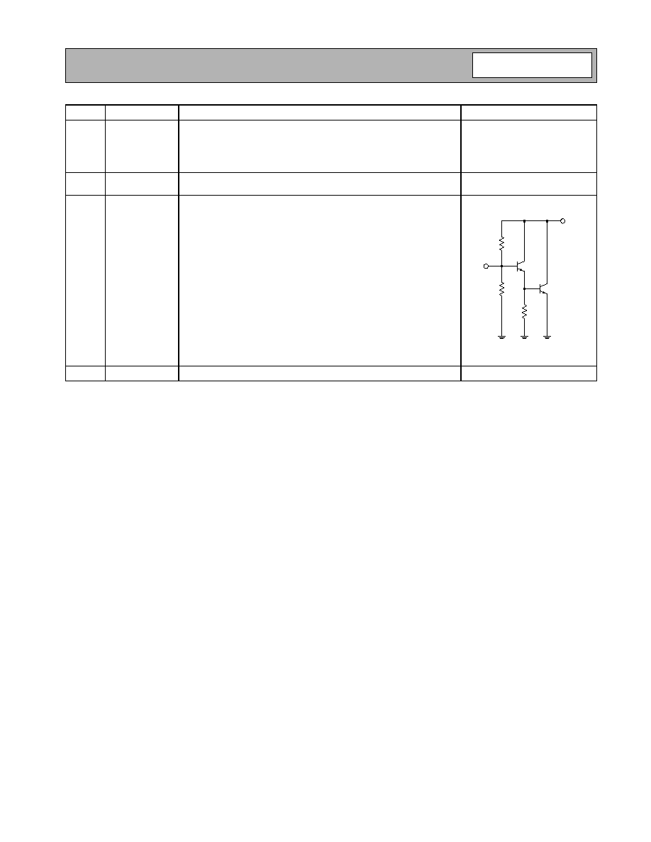
Pin
Function
Description
Interface Schematic
1
RF IN
RF input pin. This pin is NOT internally DC blocked. A DC blocking
capacitor, suitable for the frequency of operation, should be used in
most applications. DC coupling of the input is not allowed, because this
will override the internal feedback loop and cause temperature instabil-
ity.
2
GND
Ground connection. For best performance, keep traces physically short
and connect immediately to ground plane.
3
RF OUT
RF output and bias pin. Biasing is accomplished with an external series
resistor and choke inductor to V
CC
. The resistor is selected to set the
DC current into this pin to a desired level. The resistor value is deter-
mined by the following equation:
Care should also be taken in the resistor selection to ensure that the
current into the part never exceeds maximum datasheet operating cur-
rent over the planned operating temperature. This means that a resistor
between the supply and this pin is always required, even if a supply
near 5.0V is available, to provide DC feedback to prevent thermal run-
away. Because DC is present on this pin, a DC blocking capacitor, suit-
able for the frequency of operation, should be used in most
applications. The supply side of the bias network should also be well
bypassed.
4
GND
Same as pin 2.
R
V
CC
V
DEVICE
≠
(
)
I
CC
-------------------------------------------
=
RF OUT
RF IN

4-36
NBB-400
Rev A4 030912
Typical Bias Configuration
Application notes related to biasing circuit, device footprint, and thermal considerations are available on request.
Recommended Bias Resistor Values
Supply Voltage, V
CC
(V)
5
8
10
12
15
20
Bias Resistor, R
CC
(
)
22
41
122
162
222
322
C block
1
3
4
2
V
DEVICE
C block
In
Out
L choke
(optional)
R
CC
V
CC
V
D
= 3.9 V
4-37
NBB-400
Rev A4 030912
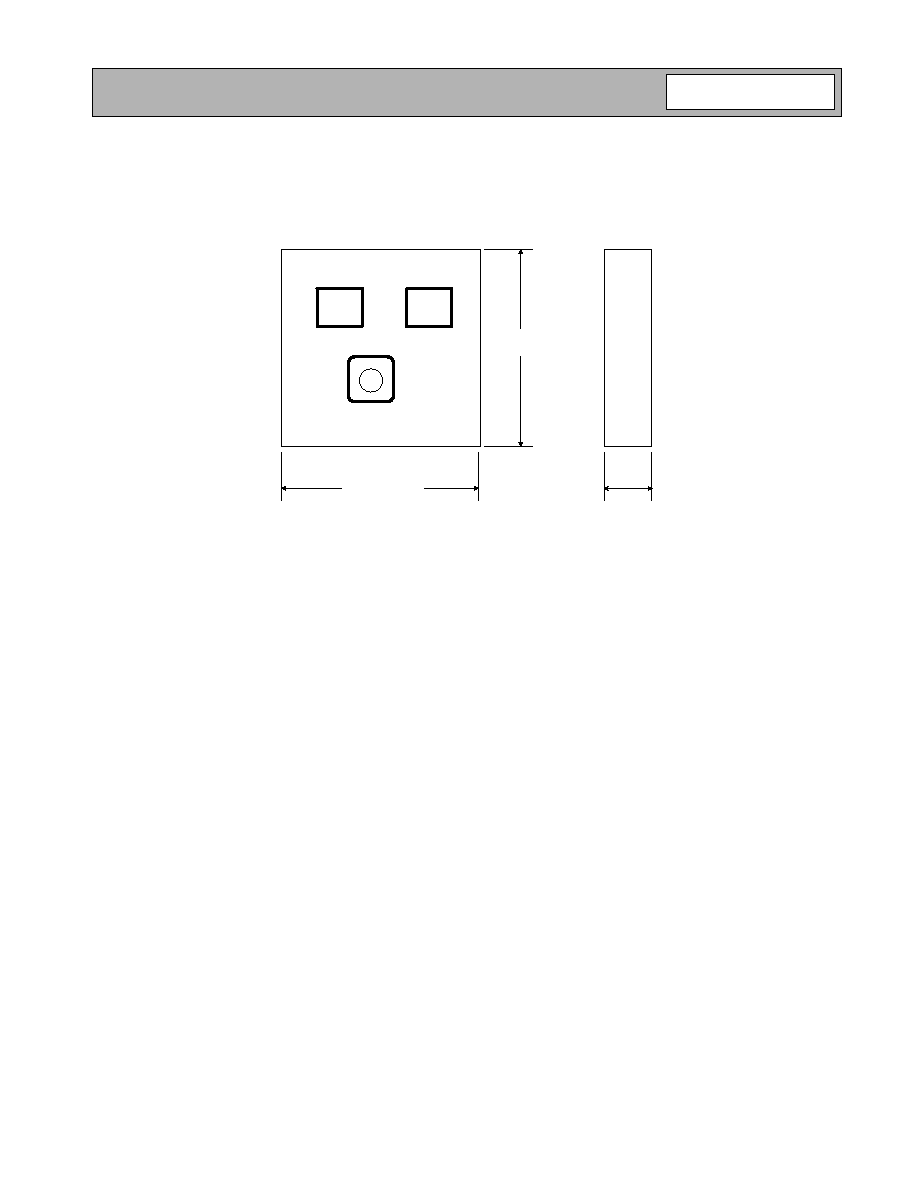
Chip Outline Drawing - NBB-400-D
Chip Dimensions: 0.017" x 0.017" x 0.004"
Sales Criteria - Unpackaged Die
Die Sales Information
∑ All segmented die are sold 100% DC-tested. Testing parameters for wafer-level sales of die material shall be nego-
tiated on a case-by-case basis.
∑ Segmented die are selected for customer shipment in accordance with RFMD Document #6000152 - Die Product
Final Visual Inspection Criteria
1
.
∑ Segmented die has a minimum sales volume of 100 pieces per order. A maximum of 400 die per carrier is allow-
able.
Die Packaging
∑ All die are packaged in GelPak ESD protective containers with the following specification:
O.D.=2"X2", Capacity=400 Die (20X20 segments), Retention Level=High(X8).
∑ GelPak ESD protective containers are placed in a static shield bag. RFMD recommends that once the bag is
opened the GelPak/s should be stored in a controlled nitrogen environment. Do not press on the cover of a closed
GelPak, handle by the edges only. Do not vacuum seal bags containing GelPak containers.
∑ Precaution must be taken to minimize vibration of packaging during handling, as die can shift during transit
2
.
Package Storage
∑ Unit packages should be kept in a dry nitrogen environment for optimal assembly, performance, and reliability.
∑ Precaution must be taken to minimize vibration of packaging during handling, as die can shift during transit
2
.
Die Handling
∑ Proper ESD precautions must be taken when handling die material.
∑ Die should be handled using vacuum pick-up equipment, or handled along the long side with a sharp pair of twee-
zers. Do not touch die with any part of the body.
∑ When using automated pick-up and placement equipment, ensure that force impact is set correctly. Excessive force
may damage GaAs devices.
INPUT
OUTPUT
GND
VIA
0.017 ± 0.001
(0.44 ± 0.03)
0.017 ± 0.001
(0.44 ± 0.03)
0.004 ± 0.001
(0.10 ± 0.03)
UNITS:
Inches
(mm)
Back of chip is ground.