 | –≠–ª–µ–∫—Ç—Ä–æ–Ω–Ω—ã–π –∫–æ–º–ø–æ–Ω–µ–Ω—Ç: RF2046 | –°–∫–∞—á–∞—Ç—å:  PDF PDF  ZIP ZIP |
¸
4-19
4
GEN
E
RA
L
P
URPO
S
E
A
M
P
L
IF
IE
RS
Preliminary
Product Description
Ordering Information
Typical Applications
Features
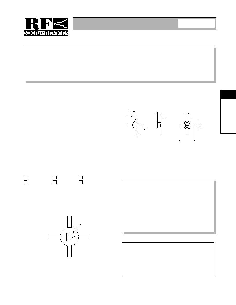
Functional Block Diagram
RF Micro Devices, Inc.
7625 Thorndike Road
Greensboro, NC 27409, USA
Tel (336) 664 1233
Fax (336) 664 0454
http://www.rfmd.com
Optimum Technology MatchingÆ Applied
Si BJT
GaAs MESFET
GaAs HBT
Si Bi-CMOS
SiGe HBT
Si CMOS
1
3
2
4
RF OUT
RF OUT
RF IN
GND
GND
MARKING - C6
RF2046
GENERAL PURPOSE AMPLIFIER
∑ Broadband, Low Noise Gain Blocks
∑ IF or RF Buffer Amplifiers
∑ Driver Stage for Power Amplifiers
∑ Final PA for Low Power Applications
∑ High Reliability Applications
∑ Broadband Test Equipment
The RF2046 is a general purpose, low cost RF amplifier
IC. The device is manufactured on an advanced Gallium
Arsenide Heterojunction Bipolar Transistor (HBT) pro-
cess, and has been designed for use as an easily-cas-
cadable 50
gain block. Applications include IF and RF
amplification in wireless voice and data communication
products operating in frequency bands up to 3000MHz.
The device is self-contained with 50
input and output
impedances and requires only two external DC biasing
elements to operate as specified. With a goal of
enhanced reliability, the extremely small Micro-X ceramic
package offers significantly lower thermal resistance than
similar size plastic packages.
∑ DC to 3000MHz Operation
∑ Internally matched Input and Output
∑ 22dB Small Signal Gain
∑ 3.8dB Noise Figure
∑ 10mW Linear Output Power
∑ Single Positive Power Supply
RF2046
General Purpose Amplifier
RF2046 PCBA
Fully Assembled Evaluation Board
4
Rev A5 010110
0.070
sq.
45∞
+ 1∞
0.055
+ 0.005
0.020
+ 0.002
0.040
+ 0.002
NOTES:
1. Shaded lead is pin 1.
2. Darkened areas are metallization.
0.200 sq.
Typ
Package Style: Micro-X Ceramic
Preliminary
4-20
RF2046
Rev A5 010110
4
GEN
E
RA
L
P
URPO
S
E
A
M
P
L
IF
IE
RS
Absolute Maximum Ratings
Parameter
Rating
Unit
Supply Current
75
mA
Input RF Power
+15
dBm
Operating Ambient Temperature
-40 to +85
∞C
Storage Temperature
-60 to +150
∞C
Parameter
Specification
Unit
Condition
Min.
Typ.
Max.
Overall
T=25 ∞C, V
D
= 3.5V, I
CC
=35mA
Frequency Range
DC to 3000
MHz
Gain
22.9
dB
Freq= 100MHz
22.2
dB
Freq= 1000MHz
18
20.8
dB
Freq=2000MHz
19.2
dB
Freq= 3000MHz
Gain Flatness
±1.1
dB
100MHz to 2000MHz
Noise Figure
3.8
dB
Freq= 2000MHz
Input VSWR
1.7:1
In a 50
system, DC to 3000MHz
Output VSWR
1.7:1
In a 50
system, DC to 3000MHz
Output IP
3
+23
dBm
Freq=2000MHz±100kHz, P
TONE
= -18dBm
Output P
1dB
+12.1
dBm
Freq=2000MHz
Reverse Isolation
23.2
dB
Freq=2000MHz
Thermal
I
CC
=35mA, P
DISS
= 120mW
Theta
JC
199
∞C/W
Maximum junction temperature
109
∞C
Mean Time Between Failures
2.0x10
4
years
T
AMB
= +85∞C
Mean Time Between Failures
1.4x10
7
years
T
AMB
= +25∞C
Mean Time Between Failures
5.3x10
11
years
T
AMB
= -40∞C
Power Supply
With 22
bias resistor
Operating Voltage
3.0
3.5
4.0
V
At pin 3 with I
CC
=35mA
Operating Current
35
mA
Caution! ESD sensitive device.
RF Micro Devices believes the furnished information is correct and accurate
at the time of this printing. However, RF Micro Devices reserves the right to
make changes to its products without notice. RF Micro Devices does not
assume responsibility for the use of the described product(s).
Preliminary
4-21
RF2046
Rev A5 010110
4
GEN
E
RA
L
P
URPO
S
E
A
M
P
L
IF
IE
RS
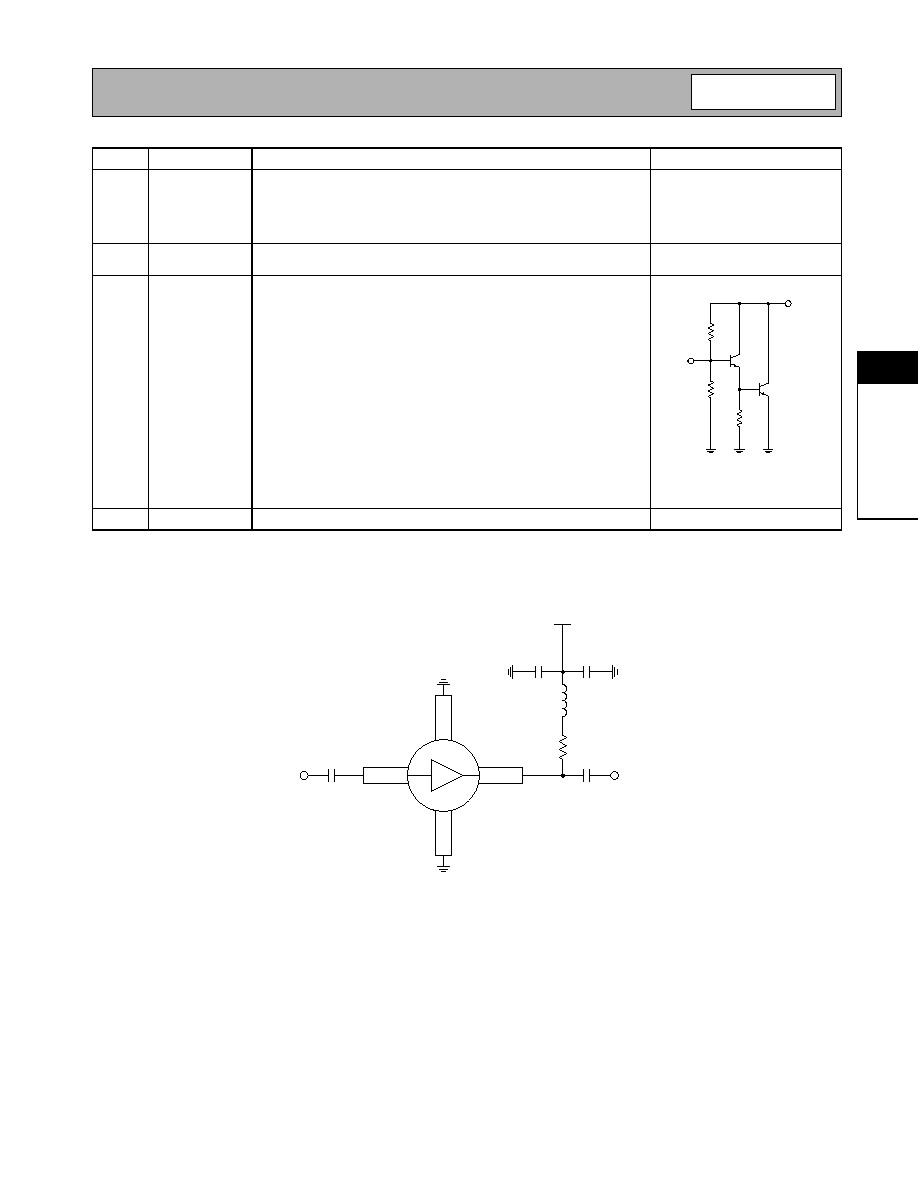
Application Schematic
Pin
Function
Description
Interface Schematic
1
RF IN
RF input pin. This pin is NOT internally DC blocked. A DC blocking
capacitor, suitable for the frequency of operation, should be used in
most applications. DC coupling of the input is not allowed, because this
will override the internal feedback loop and cause temperature instabil-
ity.
2
GND
Ground connection. Keep traces physically short and connect immedi-
ately to ground plane for best performance.
3
RF OUT
RF output and bias pin. Biasing is accomplished with an external series
resistor and choke inductor to V
CC
. The resistor is selected to set the
DC current into this pin to a desired level. The resistor value is deter-
mined by the following equation:
Care should also be taken in the resistor selection to ensure that the
current into the part never exceeds 75 mA over the planned oper-
ating temperature. This means that a resistor between the supply and
this pin is always required, even if a supply near 3.6V is available, to
provide DC feedback to prevent thermal runaway. Because DC is
present on this pin, a DC blocking capacitor, suitable for the frequency
of operation, should be used in most applications. The supply side of
the bias network should also be well bypassed.
4
GND
Same as pin 2.
R
V
SUPPL Y
V
DEVI CE
≠
(
)
I
CC
-------------------------------------------------------
=
RF OUT
RF IN
RF OUT
22 pF
R
BIAS
10 nF
22 pF
47 nH
22 pF
RF IN
V
CC
1
3
2
4
Preliminary
4-22
RF2046
Rev A5 010110
4
GEN
E
RA
L
P
URPO
S
E
A
M
P
L
IF
IE
RS
Evaluation Board Schematic
(Download Bill of Materials from www.rfmd.com.)
Evaluation Board Layout
Board Size 1.195" x 1.000"
C2
100 pF
C1
100 pF
50
µ
strip
50
µ
strip
RF OUT
J2
RF IN
J1
P1-1
NC
P1
VCC
GND
1
2
3
L1
100 nH
R1
22
VCC
P1-1
C3
100 pF
C4
1
µ
F
Drawing 204X400-
1
3
2
4

Preliminary
4-23
RF2046
Rev A5 010110
4
GEN
E
RA
L
P
URPO
S
E
A
M
P
L
IF
IE
RS
Gain versus Frequency Across Temperature
I
CC
= 35 mA
14.00
15.00
16.00
17.00
18.00
19.00
20.00
21.00
22.00
23.00
24.00
0.10
0.69
1.28
1.87
2.46
3.05
3.64
4.23
4.82
5.41
6.00
Frequency (GHz)
Gain
(dB)
-40 C
26 C
85 C
Output P1dB versus Frequency Across Temperature
I
CC
= 35 mA
10.00
11.00
12.00
13.00
14.00
15.00
16.00
0.10
0.69
1.28
1.87
2.46
3.05
3.64
4.23
4.82
5.41
6.00
Frequency (GHz)
Output
Power
(
dBm)
-40 C
26 C
85 C
Output IP3 versus Frequency Across Temperature
I
CC
= 35 mA
20.00
21.00
22.00
23.00
24.00
25.00
26.00
27.00
28.00
0.10
0.69
1.28
1.87
2.46
3.05
3.64
4.23
4.82
5.41
6.00
Frequency (GHz)
3rd
O
rder
Intercept
Power
(
dBm)
-40 C
26 C
85 C
Noise Figure versus Frequency Across Temperature
I
CC
= 35 mA
2.00
3.00
4.00
5.00
6.00
7.00
8.00
0.10
0.69
1.28
1.87
2.46
3.05
3.64
4.23
4.82
5.41
6.00
Frequency (GHz)
Noise
Figure
(
dB)
-40 C
26 C
85 C
Input VSWR versus Frequency Across Temperature
I
CC
= 35 mA
1.00
1.50
2.00
2.50
0.10
0.69
1.28
1.87
2.46
3.05
3.64
4.23
4.82
5.41
6.00
Frequency (GHz)
VSWR
-40 C
26 C
85 C
Output VSWR versus Frequency Across Temperature
I
CC
= 35 mA
1.00
1.50
2.00
2.50
0.10
0.69
1.28
1.87
2.46
3.05
3.64
4.23
4.82
5.41
6.00
Frequency (GHz)
VSWR
-40 C
26 C
85 C