¸
2-99
2
PO
W
E
R
A
M
P
LI
FI
E
R
S
Product Description
Ordering Information
Typical Applications
Features
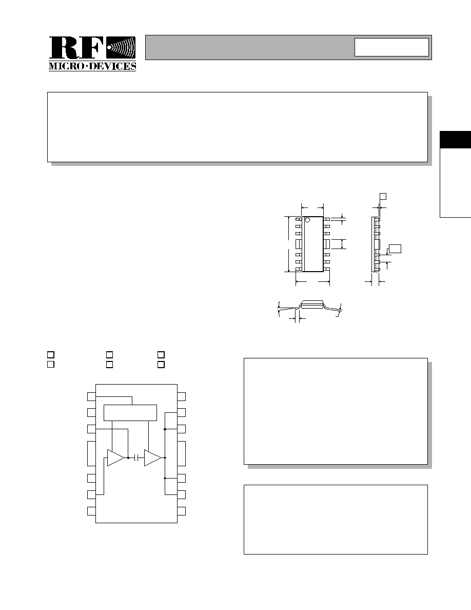
Functional Block Diagram
RF Micro Devices, Inc.
7628 Thorndike Road
Greensboro, NC 27409, USA
Tel (336) 664 1233
Fax (336) 664 0454
http://www.rfmd.com
Optimum Technology MatchingÆ Applied
Si BJT
GaAs MESFET
GaAs HBT
Si Bi-CMOS
SiGe HBT
Si CMOS
1
2
3
4
5
6
7
8
16
15
14
13
12
11
10
9
PC
NC
VCC2
GND
GND
GND1
RF IN
VCC1
NC
RF OUT
RF OUT
GND
GND
RF OUT
RF OUT
NC
BIAS
RF2131
HIGH EFFICIENCY AMPS/ETACS AMPLIFIER
∑ AMPS/ETACS Cellular Handsets
∑ CDPD Portable Data Cards
∑ 900MHz ISM Band Equipment
∑ Commercial and Consumer Systems
∑ Portable Battery-Powered Equipment
The RF2131 is a high-power, high-efficiency amplifier IC.
The device is manufactured on an advanced Gallium Ars-
enide Heterojunction Bipolar Transistor (HBT) process,
and has been designed for use as the final RF amplifier in
AMPS and ETACS handheld equipment, spread spec-
trum systems, CDPD, and other applications in the
800MHz to 950MHz band. On-board power control pro-
vides over 30dB of control range with an analog voltage
input, and provides power down with a logic "low" for
standby operation. Although it is intended for class C
operation, linear class AB operation can be achieved by
raising the bias level. The device is self-contained with
50
input and the output can be easily matched to obtain
optimum power and efficiency characteristics.
∑ Single 4.0V to 7.0V Supply
∑ 1.2W Output Power
∑ 25dB Gain With Analog Gain Control
∑ 64% Efficiency
∑ Digitally Controlled Power Down Mode
∑ 800MHz to 950MHz Operation
RF2131
High Efficiency AMPS/ETACS Amplifier
RF2131 PCBA
Fully Assembled Evaluation Board
2
Rev B4 010417
0.035
0.016
0.010
0.008
8∞ MAX
0∞ MIN
0.021
0.014
0.392
0.386
0.158
0.150
0.244
0.230
0.069
0.064
0.050
0.060
0.054
-A-
0.009
0.004
Package Style: Standard Batwing

2-100
RF2131
Rev B4 010417
2
PO
W
E
R
A
M
P
LI
FI
E
R
S
Absolute Maximum Ratings
Parameter
Rating
Unit
Supply Voltage
-0.5 to +8.5
V
DC
Power Control Voltage (V
PC
)
-0.5 to +4.5
V
DC Supply Current
570
mA
Input RF Power
+12
dBm
Output Load VSWR
10:1
Operating Case Temperature
-40 to +100
∞C
Ambient Operating Temperature
-40 to +85
∞C
Storage Temperature
-40 to +150
∞C
Parameter
Specification
Unit
Condition
Min.
Typ.
Max.
Overall
T = 25 ∞C, V
CC
= 4.8V, V
PC
set for
P
OUT
= +31dBm, Freq= 836MHz
Operating Frequency Range
824 to 849
MHz
As configured in Application schematics
Usable Frequency Range
800 to 950
MHz
Maximum CW Output Power
+30.5
+31
dBm
Depends on output matching
Total CW Efficiency
55
64
%
At Max Output
DC Current at 1.2W Output
400
mA
As configured in Application Circuit #1
Input Power for 1.2W output
+6
+8
dBm
Noise Power Output
-90
-85
dBm/30kHz
In 869 - 894 MHz band (any gain or input
power setting)
OFF Isolation
20
25
dB
V
PC
= 0V, Input Power= +6dBm
Second Harmonic
-30
-25
dBc
Depends upon external matching. Second
harmonic levels directly from the IC are
approximately 20 to 25dBc
Input VSWR
<2:1
Input Impedance
50
Power Down Control
Turn On/Off Time
100
ns
V
PC
"OFF" Voltage
0.2
0.5
V
V
PC
"ON" Voltage
3.6
4.0
V
Power Supply
Voltage
4.8
V
Specifications
Voltage
4.0
7.0
V
Operating Limits
Caution! ESD sensitive device.
RF Micro Devices believes the furnished information is correct and accurate
at the time of this printing. However, RF Micro Devices reserves the right to
make changes to its products without notice. RF Micro Devices does not
assume responsibility for the use of the described product(s).

2-101
RF2131
Rev B4 010417
2
PO
W
E
R
A
M
P
LI
FI
E
R
S
Pin
Function
Description
Interface Schematic
1
PC
Power Control. When this pin is "low", all circuits are shut off. A "low" is
typically 0.5V or less at room temperature. During normal operation
this pin is the power control. Control range varies from about 2V for
0dBm to 3.6V for +31dBm RF output power. The maximum power that
can be achieved depends on the actual output matching; see the appli-
cation information for more details.
2
NC
Not connected.
3
VCC2
Power supply for the driver stage and interstage matching. A shunt
capacitor is required for tuning the interstage to the proper frequency.
The value of this capacitor depends on the operating frequency and
power level. See the application information for details.
4
GND
Ground connection. Keep traces physically short and connect immedi-
ately to the ground plane for best performance.
5
GND
Same as pin 4.
6
GND1
Ground connection for the driver stage. Keep traces physically short
and connect immediately to the ground plane for best performance. It is
recommended to use separate vias to the ground plane for this return
path.
See pin 1 schematic.
7
RF IN
RF Input. This is a 50
input, but the actual impedance depends on the
interstage matching network connected to pin 3. An external DC block-
ing capacitor is required if this port is connected to a DC path to ground
or a DC voltage.
See pin 3 schematic.
8
VCC1
Power supply for the bias circuits. An external RF bypass capacitor is
required. Keep the traces to the capacitor as short as possible, and
connect the capacitor immediately to the ground plane.
See pin 1 schematic.
9
NC
This pin is not connected internally; however it needs to be connected
to ground externally. This will improve performance by reducing cou-
pling between pins.
10
RF OUT
RF Output and power supply for the output stage. The four output pins
are combined, and bias voltage for the final stage is provided through
these pins. The external path must be kept symmetric until combined to
ensure stability. An external matching network is required to provide the
optimum load impedance; see the application schematics for details.
11
RF OUT
Same as pin 10.
See pin 10 schematic.
12
GND
Ground connection for the output stage. Keep traces physically short
and connect immediately to the ground plane for best performance.
13
GND
Ground connection for the output stage. Keep traces physically short
and connect immediately to the ground plane for best performance.
14
RF OUT
Same as pin 10.
See pin 10 schematic.
15
RF OUT
Same as pin 10.
See pin 10 schematic.
16
NC
This pin is not connected internally, however it needs to be connected
to ground externally. This will improve performance by reducing cou-
pling between pins.
80
PC
VCC1
To Bias
Stages
RF IN
VCC2
From Bias
Stages
RF OUT
From Bias
Stages

2-102
RF2131
Rev B4 010417
2
PO
W
E
R
A
M
P
LI
FI
E
R
S
Theory of Operation and Application Information
The RF2131 is a two-stage device with 25 dB gain at
full power. Therefore, for +31dBm output power, the
drive required to fully saturate the output is +6dBm.
Based upon HBT (Heterojunction Bipolar Transistor)
technology, the part requires only a single positive
4.8 V supply to operate to full specification. Bias control
is provided through a single pin interface, and the final
stage ground is achieved through the large pins on
both sides of the package. First stage ground is
brought out through a separate ground pin for isolation
from the output. These grounds should be connected
directly with vias to the PCB ground plane. The output
is brought out through the 4 output pins, and combined
off-chip to form the RF output signal path.
The amplifier operates in Class AB bias mode. The
final stage is "deep AB", meaning the quiescent current
is very low, around 40 mA. As the RF drive is
increased, the final stage self-biases, causing the bias
point to shift up and, at full power, draws about 340mA.
The optimum load for the output stage is approximately
10
. This is the load at the output collector, and is cre-
ated by the series inductance formed by the output
bond wires, leads, and microstrip, and a shunt capaci-
tor external to the part. With this match, a 50
terminal
impedance is achieved. The input is matched to 50
with just a blocking capacitor needed. This data sheet
defines the configuration for AMPS operation, but the
output load may be modified slightly for ETACS opera-
tion. In any case the optimum load for 1.2W is the
same at the device, and only the reactive elements
must change to perform the transformation from 50
down to 10
.
The input is DC coupled; thus, a blocking cap must be
inserted in series. Also, the first stage bias may be
adjusted by a resistive divider with high value resistors
on this pin to V
PC
and ground. For nominal operation,
however, no external adjustment is necessary as inter-
nal resistors set the bias point optimally.
V
CC2
provides supply voltage to the first stage, as well
as provides some frequency selectivity to tune to the
operating band. Essentially, the bias is fed to this pin
through a short microstrip. A bypass capacitor sets the
inductance seen by the part, so placement of the
bypass cap can affect the frequency of the gain peak.
For ETACS, the capacitor placement is slightly different
than for AMPS due to the frequency shift. This supply
should be bypassed individually with 33pF or 100pF
capacitors before being combined with V
CC
for the out-
put stage to prevent feedback and oscillations.
The RF OUT pins provide the output power. Pins 10
and 11 should be combined externally with pins 14 and
15 with a symmetric combiner, as shown in the PCB
layout. Care should be taken to ensure that the output
paths are symmetric up to the point of combining. This
prevents
"odd-mode"
cancellation
from
occurring
wherein one side may get out-of-phase with the other,
affecting efficiency and stability. Bias for the final stage
is fed to this output line, and the feed must be capable
of supporting the approximately 400mA of current
required. Care should also be taken to keep the losses
low in the bias feed and output components. DC losses
in the bias choke will degrade efficiency and power.
The part will operate over a 4.0V to 4.8 V range. If, for
example, the full power is desired at minimum voltage,
then the load can be optimized at that point. This is
illustrated in Application Schematic 2. At that point, the
specified efficiency and power should be attainable. As
the voltage is increased, however, the output power will
increase. Thus, in a system design, the ALC (Auto-
matic Level Control) Loop will back down the power to
the desired level. This will occur at a less-than-opti-
mum efficiency, since the load is optimized for mini-
mum voltage. If the load is set up to optimize power
and efficiency at nominal operating voltage, then max
efficiency should be attainable there. This case is illus-
trated in Application Schematic 1. As the voltage drops
to minimum, power will degrade, but the efficiency
tends to be maintained. For nominal 31.5dBm at 4.8V
setup, as the voltage drops to 4.0V, the output power
drops to 30.5dBm with a constant V
PC
.
The HBT breakdown voltage is >20V, so nominally at
4.8 V there should be no issue with overvoltage. Under
extreme conditions, however, which can occur in a cel-
lular handset environment, the supply voltage could be
as high as 7.5 V to 8.5V. These conditions may corre-
spond to operation in a battery charger, especially with
the battery removed, which "unloads" the supply cir-
cuit. To add to this worst-case scenario, the RF drive
may be at full power during transmit, and the output
VSWR could be extremely high, corresponding to a
broken or removed antenna. Under all of the above
conditions, the peak RF voltages could well exceed two
times the supply voltage, forcing the device into break-
down. The RF2131 includes overvoltage protection
diodes at the output, which begin clipping the wave-
form peaks at approximately 15V. This protects the
device's output from breaking down under these worst-

2-103
RF2131
Rev B4 010417
2
PO
W
E
R
A
M
P
LI
FI
E
R
S
case conditions, and provides a rugged, robust compo-
nent for the system designer.
High current conditions are also potentially dangerous
to any RF device. High currents lead to high channel
temperatures and may force early failures. The
RF2131 includes temperature compensation circuits in
the bias network to stabilize the RF transistors, thus
limiting the current through the amplifier and protecting
the devices from damage. The same mechanism
works to compensate the currents due to ambient tem-
perature variations.

2-104
RF2131
Rev B4 010417
2
PO
W
E
R
A
M
P
LI
FI
E
R
S
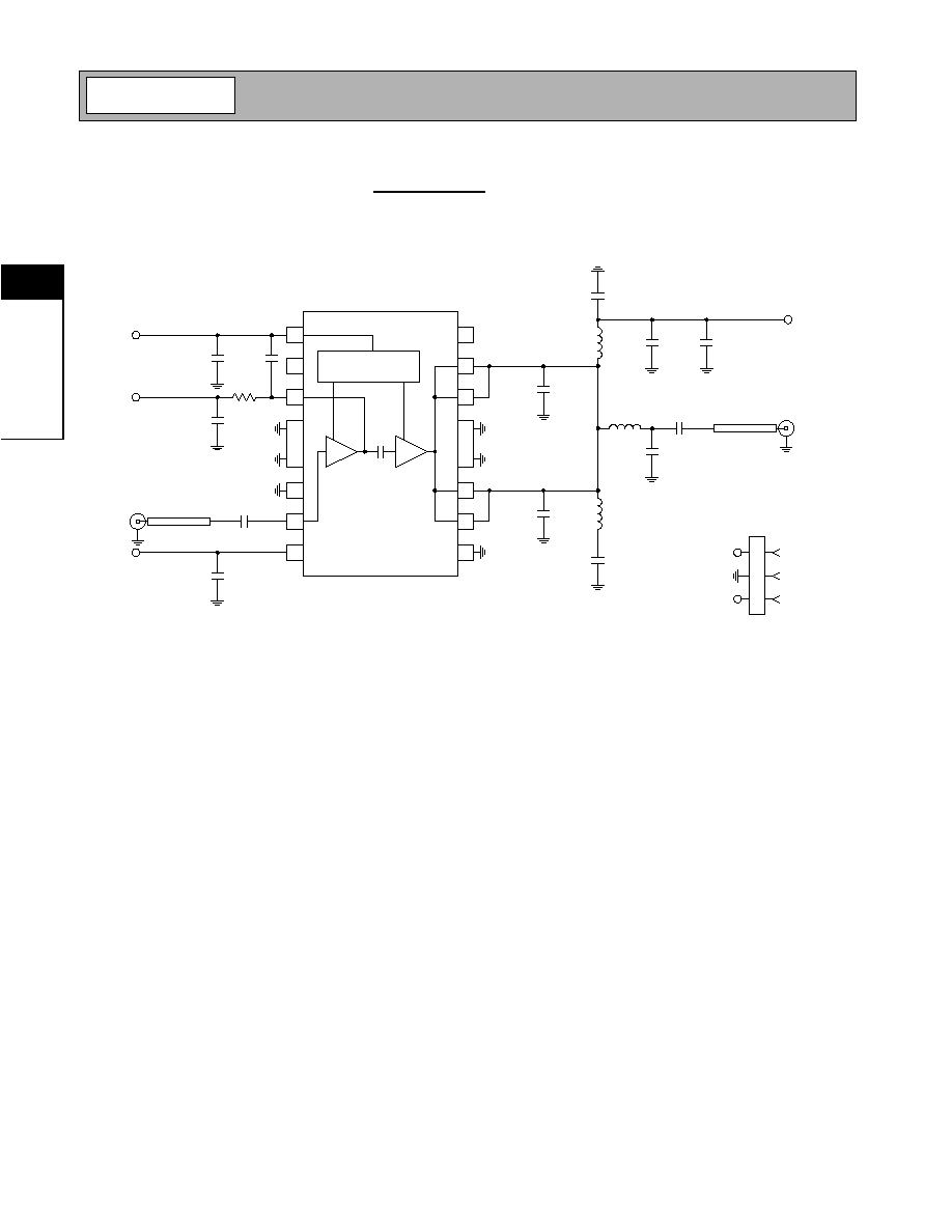
Application Schematic 1
Optimized for Efficiency at 4.8V
This schematic defines the optimum configuration for maximum efficiency at 4.8V. Under these conditions, as can be
seen in the data plots, the power drops at 4.0 V. Over 70% power-added efficiency can be achieved at +30.8 dBm with
4.8 V and +8dBm input level with this implementation.
1
2
3
4
5
6
7
8
16
15
14
13
12
11
10
9
BIAS
100 nF
100 pF
RF IN
10 nF
V
CC
10 nF
100 pF
10 nH
4.7 pF
10 nH
4.7 pF
2.7 nH
100 pF
RF OUT
5.6 pF
33 pF
V
CC
100 pF
100 nF
33 pF
V
CC
0.200"
VPC

2-105
RF2131
Rev B4 010417
2
PO
W
E
R
A
M
P
LI
FI
E
R
S
Application Schematic 2
Optimized for Power and Efficiency over 4.0V to 4.8V
This application circuit differs from Application schematic 1 only slightly in the output tuning. The output shunt capacitor
has been moved 0.060" closer to the device, and has increased from 5.6 pF to 6.2pF. This retuning allows over
+30.8dBm of output power to be achieved down to 4.0V, however a couple of percent points of efficiency are sacrificed.
This implementation is recommended for some additional margin on output power.
1
2
3
4
5
6
7
8
16
15
14
13
12
11
10
9
BIAS
100 nF
100 pF
RF IN
10 nF
V
CC
10 nF
100 pF
10 nH
4.7 pF
10 nH
4.7 pF
2.7 nH
100 pF
RF OUT
6.2 pF
33 pF
V
CC
100 pF
100 nF
33 pF
V
CC
0.140"
VPC
2-106
RF2131
Rev B4 010417
2
PO
W
E
R
A
M
P
LI
FI
E
R
S
Evaluation Board Schematic
(Download Bill of Materials from www.rfmd.com.)
1
2
3
4
5
6
7
8
16
15
14
13
12
11
10
9
BIAS
C11
100 nF
VPC
VCC
C10
10 nF
C12
10
nF
C1
100 pF
50
µ
strip
RF IN
J1
VCC
C13
100
pF
C3
4.7 pF
C4
4.7 pF
C7
33 pF
L1
2.7 nH
C5
100 pF
C2
6.2 pF
RF OUT
J2
L3
10 nH
C6
33 pF
L2
10 nH
VCC
C8
10
µ
F
C9
100 pF
50
µ
strip
2131400A
R1
0
P1-1
P1-3
P1
VCC
GND
1
2
3
PC

2-107
RF2131
Rev B4 010417
2
PO
W
E
R
A
M
P
LI
FI
E
R
S
Evaluation Board Layout
3" x 2"

2-108
RF2131
Rev B4 010417
2
PO
W
E
R
A
M
P
LI
FI
E
R
S