 | –≠–ª–µ–∫—Ç—Ä–æ–Ω–Ω—ã–π –∫–æ–º–ø–æ–Ω–µ–Ω—Ç: RF2145 | –°–∫–∞—á–∞—Ç—å:  PDF PDF  ZIP ZIP |

¸
2-141
2
PO
W
E
R
A
M
P
LI
FI
E
R
S
Product Description
Ordering Information
Typical Applications
Features
Functional Block Diagram
RF Micro Devices, Inc.
7625 Thorndike Road
Greensboro, NC 27409, USA
Tel (336) 664 1233
Fax (336) 664 0454
http://www.rfmd.com
Optimum Technology MatchingÆ Applied
Si BJT
GaAs MESFET
GaAs HBT
Si Bi-CMOS
SiGe HBT
Si CMOS
1
2
3
4
5
6
7
8
16
15
14
13
12
11
10
9
PC
GND
GND
VCC1
RF IN
GND
GND
NC
NC
GND
GND
RF OUT
RF OUT
GND
GND
NC
RF2145
DCS1800/1900 POWER AMPLIFIER
∑ 4.8V DCS1800/1900 Handsets
∑ 3V DECT Handsets and Base Stations
∑ Commercial and Consumer Systems
∑ Portable Battery Powered Equipment
The RF2145 is a high power, high efficiency amplifier IC.
The device is manufactured on an advanced Gallium Ars-
enide Heterojunction Bipolar Transistor (HBT) process,
and has been designed for use as the final RF amplifier in
a 4-cell DCS1800 or DCS1900 handset. The device is
packaged in a 16-lead plastic package with wide ground
leads, and is self-contained with the exception of the out-
put matching network and power supply feed line. Only a
single positive voltage is required to operate with full
power and efficiency, and on-board power control and
power-down functions are provided.
∑ Single 4.8V Power Supply
∑ +32dBm Output Power
∑ 28dB Small Signal Gain
∑ 55% Power Added Efficiency
∑ Power Control
∑ 1700MHz to 1900MHz Frequency Range
RF2145
DCS1800/1900 Power Amplifier
RF2145 PCBA
Fully Assembled Evaluation Board
2
Rev B5 010329
.059
.054
.050
.392
.386
.035
.016
.244
.230
8∞MAX
0∞MIN
.010
.008
.158
.150
.069
.064
1
.009
.004
.020
.014
Package Style: SOP-16 QBW1
2-142
RF2145
Rev B5 010329
2
PO
W
E
R
A
M
P
LI
FI
E
R
S
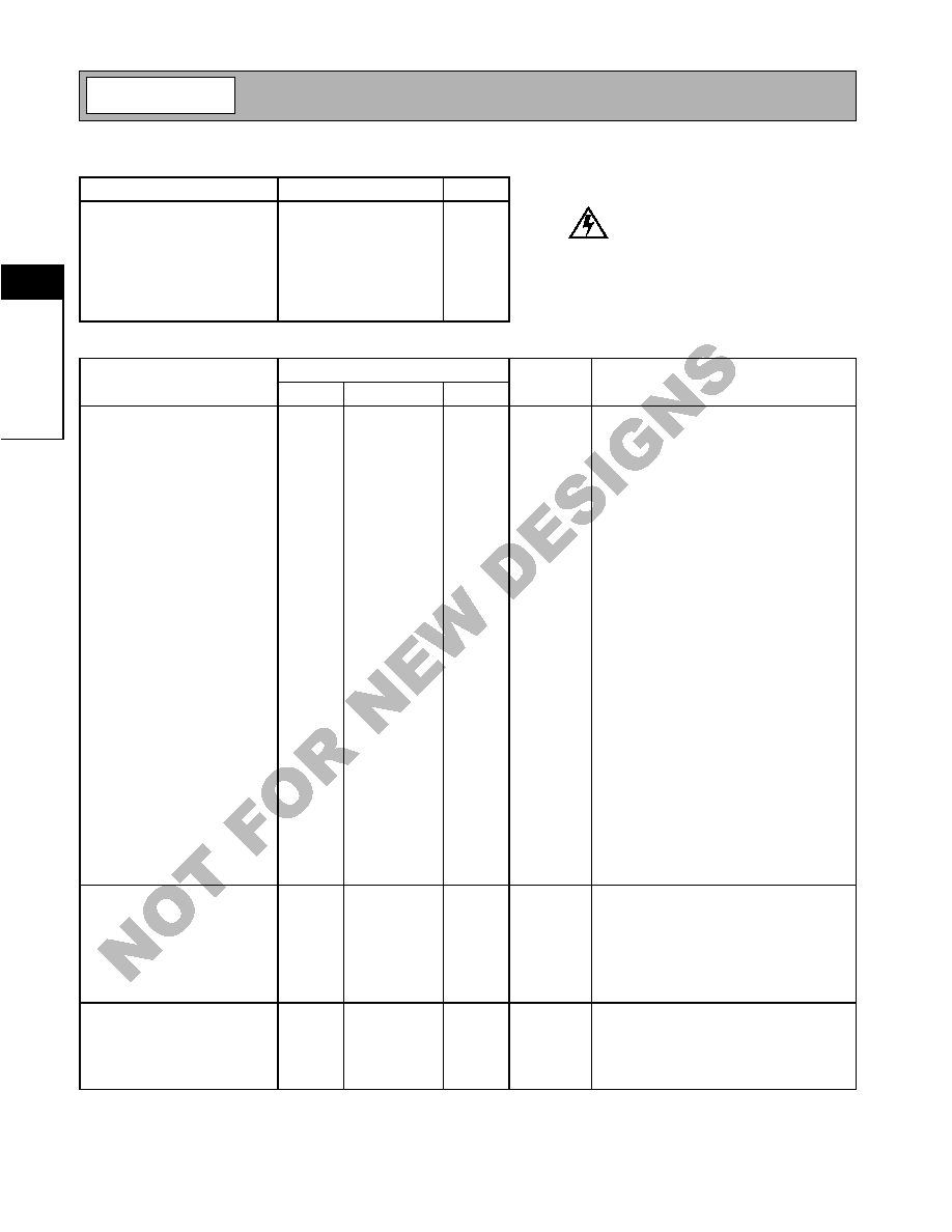
Absolute Maximum Ratings
Parameter
Rating
Unit
Supply Voltage
-0.5 to +7.5
V
DC
Power Control Voltage (V
PC
)
-0.5 to +3.0
V
DC Supply Current
675
mA
Input RF Power
+12
dBm
Output Load VSWR
5:1
Ambient Operating Temperature
-40 to +85
∞C
Storage Temperature
-40 to +150
∞C
Parameter
Specification
Unit
Condition
Min.
Typ.
Max.
Overall
T = 25 ∞C, V
CC
= 4.8V, V
PC
= 2.5V,
P
IN
=+8dBm, Freq= 1750MHz
Operating Frequency Range
1710 to 1785
1850 to 1910
MHz
Usable Frequency Range
1700 to 1990
MHz
Maximum Output Power
+32
dBm
1/8 Duty cycle with 600
µ
s pulse width
Total Efficiency
55
%
At maximum output power
Input Power for Max Output
+8
dBm
Input Intermodulation Distortion
-57
dBc
Input signal consists of F
1
at 1785MHz at
+8dBm, F
2
at 1765MHz at -42dBm. Output
power at F
1
is set to +32.5dBm. Specified
power level at 1805MHz relative to F
1
. This
refers to the amount of TX band noise which
converts into the receive band.
-48
dBc
Input signal consists of F
1
at 1785MHz at
+8dBm, F
2
at 1765MHz at -32dBm. Output
power at F
1
is set to +32.5dBm. Specified
power level at 1805MHz relative to F
1
. This
refers to the amount of TX band noise which
converts into the receive band.
Output Noise Power in Receive
Band
-137
dBm/Hz
Any gain setting
Isolation
-25
dBm
In "OFF" state, P
IN
=+8dBm
Second Harmonic
-48
dBc
Third Harmonic
<-60
dBc
Input Impedance
50
Input VSWR
3.8:1
Worst-case across the band. Using evalua-
tion board; can be different with other layouts
Output Load VSWR
3:1
Spurious<-60dBc
Power Control
Power Control "ON"
2.5
3.0
V
Threshold voltage
Power Control "OFF"
0.2
0.5
V
Threshold voltage
Current into PC Input
15
mA
In "ON" state
10
µ
A
In "OFF" state
Power Control Range
45
dB
Turn On/Off TIme
100
ns
Power Supply
Power Supply Voltage
4.8
V
Specifications
2.7
6.5
V
Operating limits
Power Supply Current
550
mA
DC Current at maximum output power
10
µ
A
V
PC
= 0.5V
Caution! ESD sensitive device.
RF Micro Devices believes the furnished information is correct and accurate
at the time of this printing. However, RF Micro Devices reserves the right to
make changes to its products without notice. RF Micro Devices does not
assume responsibility for the use of the described product(s).

2-143
RF2145
Rev B5 010329
2
PO
W
E
R
A
M
P
LI
FI
E
R
S
Pin
Function
Description
Interface Schematic
1
PC
Power control pin. This also provides power down when V
PC
is less
than +0.5V. Full power is achieved at 2.5V, and >45dB of gain control is
obtainable over the full range. Approximately 15mA current is drawn
into this pin at full power.
2
GND
Ground connection. This pin should be connected to the ground plane
through a short path and may be combined with the ground plane from
Pins 3, 6, 7, 10, 11, 14, and 15. All four of these wide leads are tied
together internally to provide a low-inductance and low thermal resis-
tance path to external ground. Ground vias should be placed as close
as possible to each ground lead.
3
GND
Same as pin 2.
4
VCC1
Power supply pin for the first stage. Also provides tuning for interstage
match.
5
RF IN
RF input. This input is DC coupled, so an external blocking capacitor is
required if this pin is connected to a DC path.
See pin 4 schematic.
6
GND
Same as pin 2.
7
GND
Same as pin 2.
8
NC
No connection.
9
NC
No connection.
10
GND
Same as pin 2.
11
GND
Same as pin 2.
12
RF OUT
RF output pin. Bias is also fed to the final stage through this wide lead.
External matching is most easily achieved with a series transmission
line and shunt capacitors, as shown in the application schematic.
13
RF OUT
Same as pin 12.
14
GND
Same as pin 2.
15
GND
Same as pin 2.
16
NC
No connection.
PC
To RF
Stages
RF IN
VCC1
From Bias
Stages
RF OUT
From Bias
Stages
2-144
RF2145
Rev B5 010329
2
PO
W
E
R
A
M
P
LI
FI
E
R
S
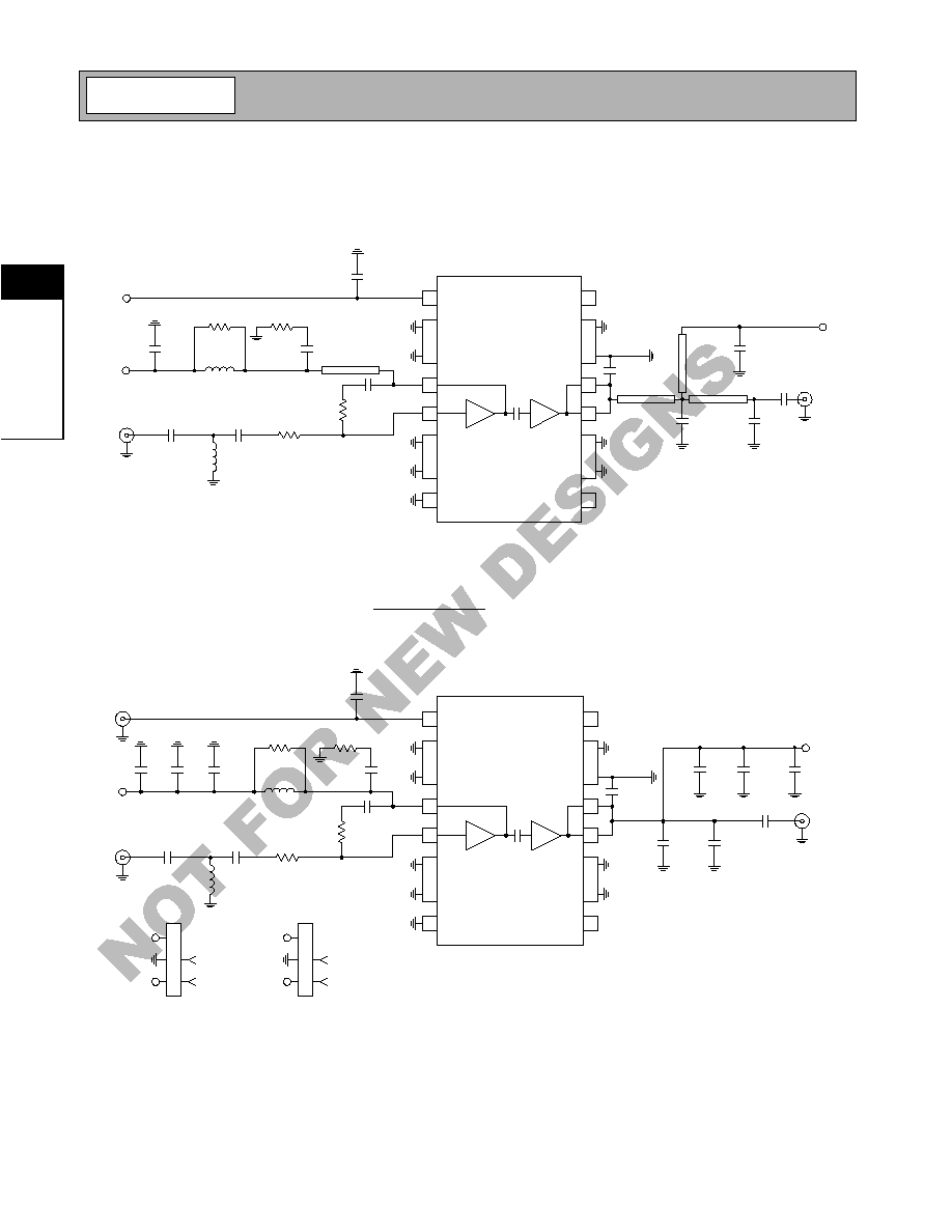
Application Schematic
DCS 1800
Evaluation Board Schematic
(Download Bill of Materials from www.rfmd.com.)
1
2
3
4
5
6
7
8
16
15
14
13
12
11
10
9
18
33 pF
2.7 nH
RF IN
33 pF
VCC2
22 nH
470
2.0 pF
PC
470 pF
33 pF
3.0 pF
3.3 pF
VCC
RF OUT
1.1 pF
3
33 pF
100 pF
270
33 pF
50
µ
strip
50
µ
strip
50
µ
strip
µ
strip
1
2
3
4
5
6
7
8
16
15
14
13
12
11
10
9
R1
18
C8
33 pF
L1
2.7 nH
RF IN
J1
C1
33 pF
VCC2
L2
22 nH
R2
470
C5
2.0 pF
C10
1 nF
C2
1
µ
F
C6
470 pF
C4
33 pF
C26
3.0 pF
C25
1 nF
C29
3.3 pF
VCC
RF OUT
J2
C23
10
µ
F
C9
1.1 pF
R4
3
C13
33 pF
C7
100 pF
R3
270
C12
33 pF
PC
J1
NC
P1-3
P1
GND
1
2
3
VCC
NC
P2-3
P2
GND
1
2
3
VCC2
2145400-

2-145
RF2145
Rev B5 010329
2
PO
W
E
R
A
M
P
LI
FI
E
R
S
Evaluation Board Layout
2" x 2"

2-146
RF2145
Rev B5 010329
2
PO
W
E
R
A
M
P
LI
FI
E
R
S