!
NO
T FOR NEW DESIGNS
2-155
2
PO
WER
AMPLI
F
I
E
RS
Product Description
Ordering Information
Typical Applications
Features
Functional Block Diagram
RF Micro Devices, Inc.
7625 Thorndike Road
Greensboro, NC 27409, USA
Tel (336) 664 1233
Fax (336) 664 0454
http://www.rfmd.com
Optimum Technology MatchingÆ Applied
Si BJT
GaAs MESFET
GaAs HBT
Si Bi-CMOS
SiGe HBT
Si CMOS
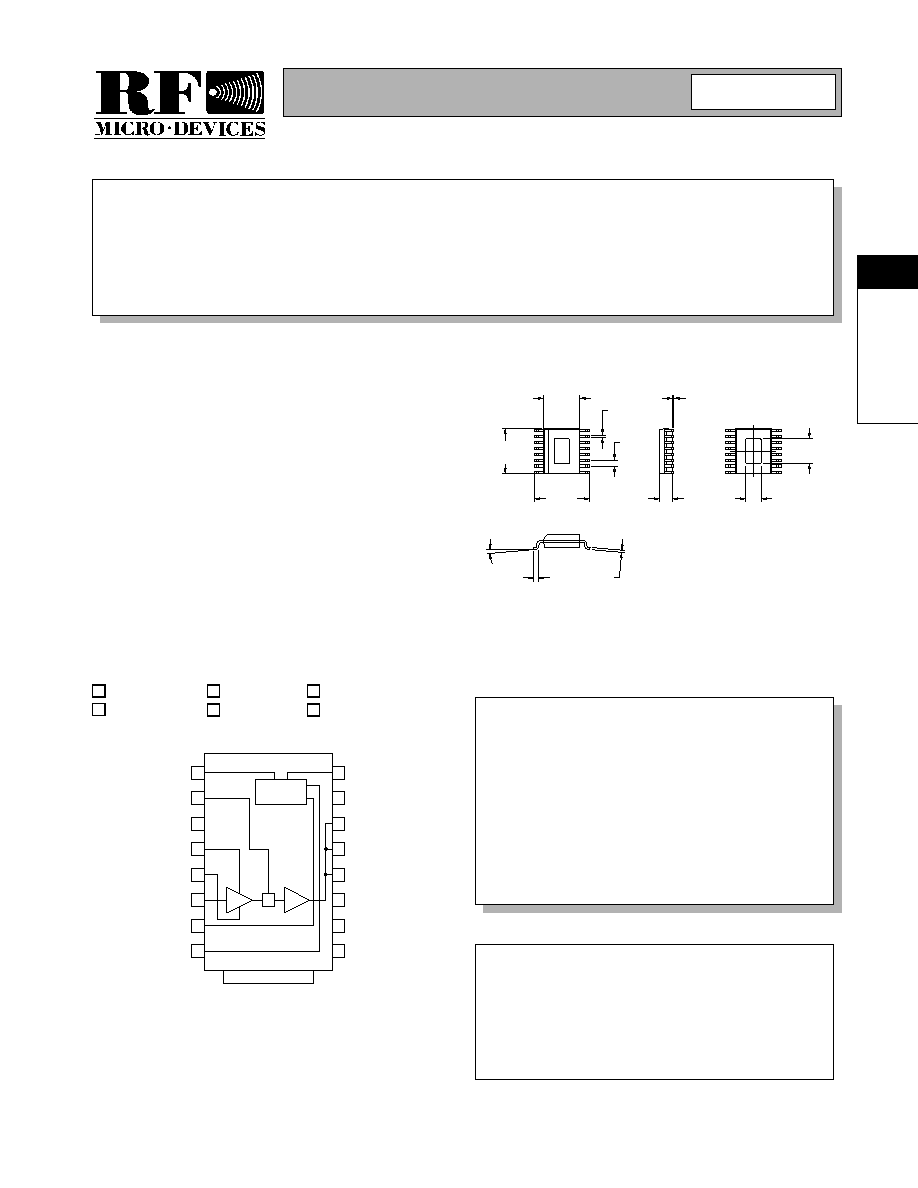
1
2
3
4
5
6
7
8
16
15
14
13
12
11
10
9
VCC
LTUNE
NC
VCC1
GND1
RF IN
VPD
VPD
MODE
NC
RF OUT
RF OUT
RF OUT
NC
NC
NC
BIAS
CIRCUITS
PACKAGE BASE
GND
RF2152
DUAL-MODE CDMA/AMPS OR TDMA/AMPS
3V POWER AMPLIFIER
∑ 3V CDMA/AMPS Cellular Handsets
∑ 3V JCDMA/TACS Cellular Handsets
∑ 3V TDMA/AMPS Cellular Handsets
∑ Spread-Spectrum Systems
∑ CDPD Portable Data Cards
∑ Portable Battery-Powered Equipment
The RF2152 is a high-power, high-efficiency linear ampli-
fier IC targeting 3V handheld systems. The device is
manufactured on an advanced Gallium Arsenide Hetero-
junction Bipolar Transistor (HBT) process, and has been
designed for use as the final RF amplifier in dual-mode
3 V CDMA/AMPS handheld digital cellular equipment,
spread-spectrum systems, and other applications in the
800MHz to 950MHz band. The device is self-contained
with 50
input and the output can be easily matched to
obtain optimum power, efficiency, and linearity character-
istics. The package is a PSSOP-16 with backside ground.
∑ Single 3V Supply
∑ 28dBm Linear Output Power
∑ 30dB Linear Gain
∑ 35% Linear Efficiency
∑ On-board Power Down Mode
∑ 800MHz to 960MHz Operation
RF2152
Dual-Mode CDMA/AMPS or TDMA/AMPS 3V Power
Amplifier
RF2152 PCBA-N Fully Assembled Evaluation Board 824-849MHz
RF2152 PCBA-J
Fully Assembled Evaluation Board 877-924MHz
2
Rev A8 001109
.059
.051
.197
.189
.244
.228
.030
.018
8 ∞MAX
0∞MIN
.009
.008
.157
.150
.012
.008
1
EXPOSED
HEATSINK
.003
.001
.025
.062
.070
.102
.110
Refer to "Handling of PSOP and PSSOP Products" on page 16-15
for special handling information.
Package Style: PSSOP-16
See
Upg
ra
ded
P
rod
ucts
RF
216
2/R
F2
192
2-156
RF2152
Rev A8 001109
2
PO
WER
AMPLI
F
I
E
RS
NO
T FOR NEW DESIGNS
See
Upg
ra
ded
P
rod
ucts
RF
216
2/R
F2
192
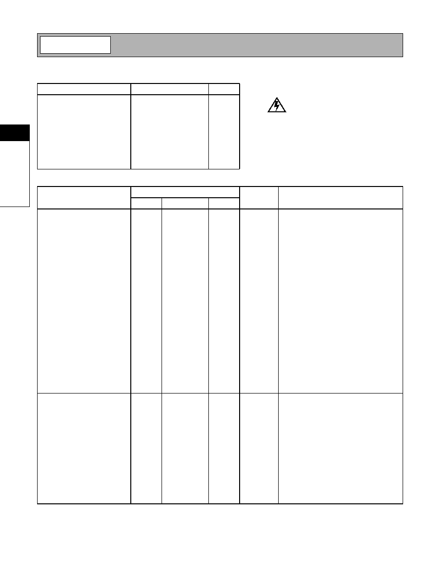
Absolute Maximum Ratings
Parameter
Rating
Unit
Supply Voltage (RF off)
+8.0
V
DC
Supply Voltage (P
OUT
31dBm)
+5.2
V
DC
DC Supply Current
1.0
A
Mode Voltage (V
MODE
)
+3.0
V
DC
Control Voltage (V
PD
)
+3.0
V
DC
Input RF Power
+12
dBm
Operating Ambient Temperature
-40 to +85
∞C
Storage Temperature
-40 to +150
∞C
Moisture Sensitivity
JEDEC LEVEL 5
Parameter
Specification
Unit
Condition
Min.
Typ.
Max.
Overall
T = 25∞C, V
CC
= 3.4V, V
PD
= 2.8V,
Freq=824MHz to 849MHz, unless otherwise
specified
Usable Frequency Range
800
960
MHz
Typical Frequency Range
824-849
877-925
MHz
MHz
Linear Gain
28
30
33
dB
Pout=28dBm
Second Harmonic (including
second harmonic trap)
-32
-38
-42
dBc
Max CW Output Power
31
31.5
32
dBm
Tuned for CDMA
Total Efficiency (AMPS mode)
40
45
55
%
Maximum Linear Output Power
(CDMA Modulation)
28
28.5
29
dBm
Tuned for CDMA
Total Linear Efficiency
30
35
38
%
Adjacent Channel Power Rejec-
tion
-44
-46
-50
dBc
ACPR@885kHz
Adjacent Channel Power Rejec-
tion
-56
-58
-62
dBc
ACPR@1980kHz
Input VSWR
< 2:1
Output Load VSWR
10:1
No oscillations
Noise Figure
5.9
6.0
6.1
dB
V
CC
= 3.4V
Noise Power P
OUT
=15dBm
P
OUT
=28dBm
P
OUT
=31dBm
86.5
89.3
92.3
dBm
dBm
dBm
V
CC
= 3.4V; 30KHz BW; RX Band NP mea-
sured from TX center band to RX center
band
Power Supply
Power Supply Voltage
3.0
3.4
5.2
V
Idle current
90
mA
MODE = low Pin 16=Ground AMPS/Low
Power CDMA Modes
Idle current
200
mA
MODE = high Pin 16=2.8V High Power
CDMA Mode (Pout>20dBm)
V
PD
current
10
mA
Pins7,8, Vpd=2.8V (Pin 7 typ. not connected,
I=5mA for Pin 8)
Turn On/Off time
<100
ns
Total Current (Power down)
10
µ
A
V
PD
= low
V
PD
"Low" Voltage
0
0.2
V
V
PD
"High" Voltage
2.7
2.8
2.9
V
MODE "High" Voltage
2.1
2.8
2.9
MODE "Low" Voltage
0
0.5
Caution! ESD sensitive device.
RF Micro Devices believes the furnished information is correct and accurate
at the time of this printing. However, RF Micro Devices reserves the right to
make changes to its products without notice. RF Micro Devices does not
assume responsibility for the use of the described product(s).
Refer to "Handling of PSOP and PSSOP Products"
on page 16-15 for special handling information.
2-157
RF2152
Rev A8 001109
2
PO
WER
AMPLI
F
I
E
RS
NO
T FOR NEW DESIGNS
See
Upg
ra
ded
P
rod
ucts
RF
216
2/R
F2
192
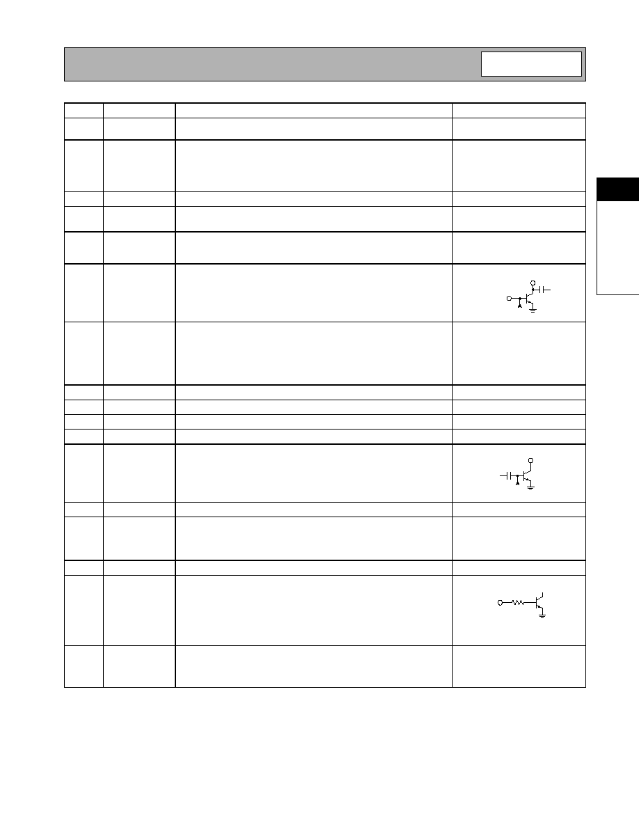
Pin
Function
Description
Interface Schematic
1
VCC
Power supply for input bias circuitry. A 100 pF high frequency bypass
capacitor is recommended.
2
LTUNE
Interstage tuning. This pin will connect to a shunt inductor used for
interstage tuning. For 824MHz to 849MHz a 1.5nH discrete inductor is
used; for 877MHz to 925MHz a shorted transmission line presenting
0.7 nH of inductance or discrete inductor may be used. This inductor
should be placed as close to the pin as possible.
3
NC
No connection. Grounding pin is recommended.
4
VCC1
Power supply for stage 1. V
CC
should be fed through a 25nH or greater
inductor with a decoupling capacitor on the V
CC
side.
See pin 6.
5
GND1
Ground for stage 1. Keep traces physically short and connect immedi-
ately to ground plane for best performance. This ground should be iso-
lated from the backside ground contact.
See pin 6.
6
RF IN
RF input. An external DC blocking capacitor is required if this port is
connected to a DC path to ground or a DC voltage.
7
VPD
Power Down control. When this pin is "low", all circuits are shut off.
When this pin is 2.8 volts, all circuits are operating normally. V
PD
requires a regulated 2.8 V for the amplifier to operate properly over all
specified temperature and voltage ranges. A dropping resistor from a
higher regulated voltage may be used to provide the required 2.8 V. A
100 pF high frequency bypass capacitor is recommended.
8
VPD
Connect to pin 7.
9
NC
No connection. Grounding pin is recommended.
10
NC
No connection. Grounding pin is recommended.
11
NC
No connection. Grounding pin is recommended.
12
RF OUT
RF output and power supply for the output stage. The bias for the out-
put stage is provided through this pin and pin 13. An external matching
network is required to provide the optimum load impedance; see the
application schematics for details. The first shunt cap of the matching
circuit should be placed as close to the pin as possible.
13
RF OUT
Same as pin 12.
See pin 12.
14
RF OUT
Harmonic trap. This pin connects to the RF output but is used for pro-
viding a low impedance to the second harmonic of the operating fre-
quency. An inductor or transmission line resonating with a shunt
capacitor at 2f
0
is connected to this pin.
See pin 12.
15
NC
No connection. Grounding pin is recommended.
16
MODE
The mode pin allows higher efficiency operation in AMPS and low
power CDMA modes. MODE should be set "low" for highest efficiency
in AMPS/TACS and in low power (<+15 dBm) CDMA operation. MODE
should be set "high" for best linearity in high power CDMA operation.
Pkg
Base
GND
Ground connection. The backside of the package should be soldered to
a top side ground pad which is connected to the ground plane with mul-
tiple vias. The pad should have a short thermal path to the ground
plane.
GND1
RF IN
VCC1
From Bias
Stages
RF OUT
From Bias
Stages
MODE

2-158
RF2152
Rev A8 001109
2
PO
WER
AMPLI
F
I
E
RS
NO
T FOR NEW DESIGNS
See
Upg
ra
ded
P
rod
ucts
RF
216
2/R
F2
192
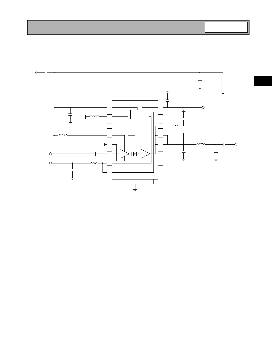
Application Schematic
824MHz to 849MHz
1
2
3
4
5
6
7
8
16
15
14
13
12
11
10
9
BIAS
CIRCUITS
R3
VPD
100 pF
100 pF
1.2
nH
47 nH
100 pF
V
CC
1 nH
2 pF
9 pF
7 pF
100 pF
RF
OUT
MODE
100 pF
100 pF
100 pF
∑L6 may be implemented as a transmission
line to reduce DC losses.
∑R3 is used for bias adjustment. 0
for 2.8 V
regulated supply.
∑All unused pins should be grounded to PC
board if possible.
20 nH
2.7 nH
PACKAGE BASE
RF IN
2-159
RF2152
Rev A8 001109
2
PO
WER
AMPLI
F
I
E
RS
NO
T FOR NEW DESIGNS
See
Upg
ra
ded
P
rod
ucts
RF
216
2/R
F2
192
Application Schematic
877MHz to 924MHz
1
2
3
4
5
6
7
8
16
15
14
13
12
11
10
9
BIAS
CIRCUITS
R3
VPD
100 pF
100 pF
RF IN
0.7 nH
47 nH
100 pF
V
CC
1 nH
2 pF
6 pF
100 pF
RF OUT
MODE
100 pF
100 pF
100 pF
∑L6 may be implemented as a transmission
line to reduce DC losses.
∑R3 is used for bias adjustment. 0
for 2.8 V
regulated supply.
∑All unused pins should be grounded to PC
board if possible.
20 nH
8 pF
2.2 nH
PACKAGE BASE