
¸
2-187
2
PO
W
E
R
A
M
P
LI
FI
E
R
S
Product Description
Ordering Information
Typical Applications
Features
Functional Block Diagram
RF Micro Devices, Inc.
7625 Thorndike Road
Greensboro, NC 27409, USA
Tel (336) 664 1233
Fax (336) 664 0454
http://www.rfmd.com
Optimum Technology MatchingÆ Applied
Si BJT
GaAs MESFET
GaAs HBT
Si Bi-CMOS
SiGe HBT
Si CMOS
4
VPD2
3
MODE
2
VPD1
13
NC
14
NC
15
NC
16
RF
I
N
1
GN
D
10
VCC
11
VCC1
12
VCC1
5
GN
D
6
NC
7
RF
O
U
T
8
RF
O
U
T
9
GN
D
RF2157
PCS CDMA/TDMA 3V POWER AMPLIFIER
∑ 3V 1850-1910MHz CDMA PCS Handsets
∑ 3V 1750-1780MHz CDMA PCS Handsets
∑ 3V TDMA PCS Handsets
∑ Spread-Spectrum Systems
∑ Commercial and Consumer Systems
∑ Portable Battery-Powered Equipment
The RF2157 is a high-power, high-efficiency linear ampli-
fier IC targeting 3V handheld systems. The device is
manufactured on an advanced Gallium Arsenide Hetero-
junction Bipolar Transistor (HBT) process, and has been
designed for use as the final RF amplifier in dual-mode
3 V CDMA and TDMA handheld digital equipment,
spread-spectrum systems, and other applications in the
1710 MHz to 1910 MHz band. The device is packaged in a
compact 4mmx4 mm LCC, as well as a 4 mmx4mm MLF
(micro leaded package). The frequency response can be
optimized for linear performance over 1710MHz to
1910 MHz. The device features a digital mode switch
which can be used to minimize operating current under
low output power conditions.
∑ Single 3V Supply
∑ 29dBm Linear Output Power
∑ 24dB Linear Gain
∑ 35% Linear Efficiency
∑ On-board Power Down Mode
∑ 1750MHz to 1910MHz Operation
RF2157
PCS CDMA Power Amplifier
RF2157 PCBA
Fully Assembled Evaluation Board
2
Rev A19 010611
3.75
3.75
+
1.50 SQ
4.00
4.00
1
0.45
0.28
3.20
1.60
0.75
0.50
12∞
INDEX AREA 3
1.00
0.90
0.75
0.65
0.05
0.00
NOTES:
5
Package Warpage: 0.05 max.
4
Pins 1 and 9 are fused.
Shaded Pin is Lead 1.
1
Dimension applies to plated terminal and is measured between
0.10 mm and 0.25 mm from terminal tip.
2
The terminal #1 identifier and terminal numbering convention
shall conform to JESD 95-1 SPP-012. Details of terminal #1
identifier are optional, but must be located within the zone
indicated. The identifier may be either a mold or marked
feature.
3
0.80
TYP
2
1
Dimensions in mm.
Package Style: LCC, 16-Pin, 4x4
2-188
RF2157
Rev A19 010611
2
PO
W
E
R
A
M
P
LI
FI
E
R
S
Caution! ESD sensitive device.
RF Micro Devices believes the furnished information is correct and accurate
at the time of this printing. However, RF Micro Devices reserves the right to
make changes to its products without notice. RF Micro Devices does not
assume responsibility for the use of the described product(s).
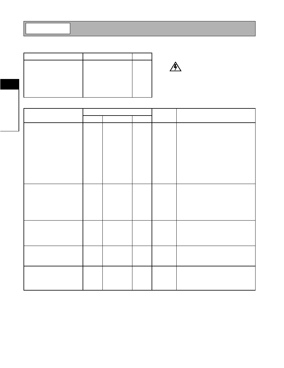
Absolute Maximum Ratings
Parameter
Rating
Unit
Supply Voltage (RF off)
+8.0
V
DC
Supply Voltage (P
OUT
31dBm)
+4.5
V
DC
Mode Voltage (V
MODE
)
+3.5
V
DC
Control Voltage (V
PD
)
+3.5
V
DC
Input RF Power
+12
dBm
Operating Case Temperature
-30 to +110
∞C
Storage Temperature
-65 to +150
∞C
Parameter
Specification
Unit
Condition
Min.
Typ.
Max.
Overall
T = 25∞C, V
CC
= 3.4 V, V
PD
= 2.8V,
P
OUT
=29dBm, unless otherwise specified
Usable Frequency Range
1750
1910
MHz
Typical Frequency Range
1750-1780
1850-1910
MHz
MHz
Tuned Matching Network
Tuned Matching Network
Linear Gain
23
25
28
dB
P
OUT
=29dBm, V
MODE
0.5V
22
24
26
dB
P
OUT
=29dBm, V
MODE
2.5V
Small Signal Gain
22
27
29
dB
P
IN
-20dBm
Second Harmonic (Including
second harmonic trap)
-35
dBc
Third Harmonic
-40
dBc
Fourth Harmonic
-45
dBc
CDMA
V
MODE
2.5V
Linear Output Power
29
dBm
28
dBm
V
CC
= 3.0V
Linear Efficiency
33
37
%
6
P
OUT
=16dBm
CDMA ACPR @ 1.25MHz
-46
-44
dBc
Noise Power @ 80MHz Offset
-139
dBm/Hz
CDMA
V
MODE
0.5V
Linear Output Power
29
dBm
Linear Efficiency
30
35
%
CDMA ACPR @ 1.25MHz
-46
-44
dBc
Noise Power @ 80MHz Offset
-139
dBm/Hz
TDMA
Linear Efficiency
30
37
%
TDMA ACPR @ 30kHz Offset
-31
-28
dBc
TDMA ACPR @ 60kHz Offset
-52
-48
dBc
Input VSWR
< 2:1
Output Load VSWR
10:1
No damage.
Stability
5:1
Junction to Case
Thermal Resistance
25
∞C/W
2-189
RF2157
Rev A19 010611
2
PO
W
E
R
A
M
P
LI
FI
E
R
S
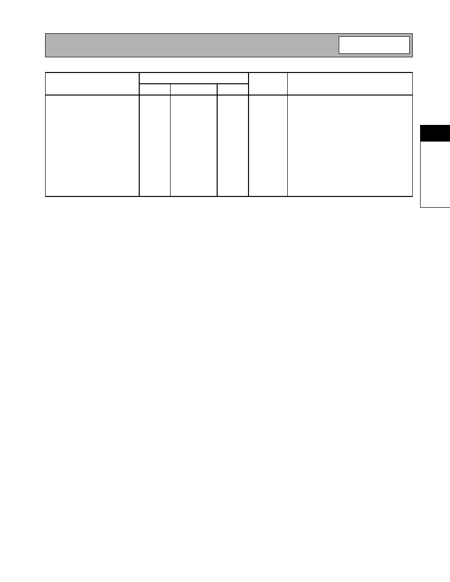
Parameter
Specification
Unit
Condition
Min.
Typ.
Max.
Power Supply
Power Supply Voltage
3.4
4.5
V
Idle Current
325
mA
V
MODE
0.5V
110
140
175
mA
V
MODE
= 2.8V
V
PD
Current
7
9
mA
V
CC
= 3.4V, V
PD
= 2.8V, V
MODE
=2.8V
No RF input power applied.
Turn On/Off Time
100
ns
Total Current (Power Down)
10
µ
A
V
PD
0.2V
V
PD
Low Voltage
0
0.2
V
V
PD
High Voltage
2.7
2.8
2.9
V
MODE High Voltage
2.5
2.8
R
1
= 1k
MODE Low Voltage
0
0.5

2-190
RF2157
Rev A19 010611
2
PO
W
E
R
A
M
P
LI
FI
E
R
S
Pin
Function
Description
Interface Schematic
1
GND
This pin is internally grounded to the die flag.
2
VPD1
Power down control for first stage. When this pin is "low", first stage cir-
cuits are shut off. When this pin is 2.8V, all first stage circuits are oper-
ating normally. V
PD1
requires a regulated 2.8V for the amplifier to
operate properly over all specified temperature and voltage ranges. A
dropping resistor from a higher regulated voltage may be used to pro-
vide the required 2.8V.
3
MODE
For full power operation, VMODE is set low. VMODE will reduce the
bias current by approximately 50% when set HIGH. Large Signal Gain
is reduced approximately 1.5dB at 29dBm P
OUT
. Small Signal Gain is
reduced by approximately 6dB at lower temperatures. An external
series resistor is optional to limit the amount of current required.
4
VPD2
Power down control for the second stage. When this pin is "low", the
second stage circuit is shut off. When this pin is 2.8V, the second stage
circuit is operating normally. V
PD
requires a regulated 2.8V for the
amplifier to operate properly over all specified temperature and voltage
ranges. A dropping resistor from a higher regulated voltage may be
used to provide the required 2.8V. A 15pF high frequency bypass
capacitor is recommended.
5
GND
Connect to ground plane via 15nH inductor. DC return for the second
stage bias circuit.
6
NC
This pin is internally a no connection. It is recommended that this pin
be connected to either the RF output matching network or to the
ground plane.
7
RF OUT
RF output and power supply for final stage. This is the unmatched col-
lector output of the second stage. A DC block is required following the
matching components. The biasing may be provided via a parallel L-C
set for resonance at the operating frequency of 1710MHz to 1910MHz.
It is important to select an inductor with very low DC resistance with a
1A current rating. Alternatively, shunt microstrip techniques are also
applicable and provide very low DC resistance. Low frequency bypass-
ing is required for stability.
8
RF OUT
Same as pin 7.
See pin 7.
9
GND
This pin is internally grounded to the die flag.
10
VCC
Supply for bias reference and control circuits. High frequency bypass-
ing may be necessary.
11
VCC1
Power supply for first stage and interstage match. Pins 11 and 12
should be connected by a common trace where the pins contact the
printed circuit board.
12
VCC1
Same as pin 11.
13
NC
This pin is internally a no connection. It is recommended that this pin
be connected to either VCC1 or to the ground plane.
14
NC
It is recommended that these pins be connected to the ground plane for
improved isolation between RF IN (pin 16) and the VCC1 pins (pins 11
and 12).
15
NC
It is recommended that these pins be connected to the ground plane for
improved isolation between RF IN (pin 16) and the VCC1 pins (pins 11
and 12).
16
RF IN
RF input. An external 15pF series capacitor is required as a DC block.
In addition, a series transmission line and shunt capacitor, 5pF, are
required to provide 2:1 VSWR.
Pkg
Base
GND
Ground connection. The backside of the package should be soldered to
a top side ground pad which is connected to the ground plane with mul-
tiple vias. The pad should have a short thermal path to the ground
plane.
RF OUT
From Bias
Network
GND1
RF IN
VCC1
From
Bias
Stages
15 pF
5 pF

2-191
RF2157
Rev A19 010611
2
PO
W
E
R
A
M
P
LI
FI
E
R
S
Application Schematic
Korea - CDMA
15
16
1
2
3
4
12
11
10
9
8
7
6
5
14
13
C24
4.7 pF
C5
15 pF
RF IN
TL
4
C14 (pF)
C30 (pF)
C1 (pF)
L1 (nH)
2.2
10
4.7
12
CDMA (Korea)
Board
C1
4.7 pF
C14
2.2 pF
C3
15 pF
RF OUT
L1
12 nH
C7
1.5 pF
C4
15 pF
C28
10 nF
* L1 is a High Q inductor (i.e., Coilcraft 0805HQ-series).
**C1 and C14 are High Q capacitors (i.e., Johanson C-series).
Pins 1 and 9 are internally grounded to the die flag.
TL
1
TL
2
CDMA (Korea)
Transmission
Line Length
TL
1
30-40 mils
150 mils
20-30 mils
TL
2
TL
3
200 mils
TL
4
C27
15 pF
R12
Jumper
VREG
R1
1 k
VMODE
L4
15 nH
C13
15 pF
R11
Jumper
C6
15 pF
VCC
C30
11 pF
L2
8.2 nH
C8
10 nF
RF Choke - Bias inductor
for the amplifier interstage
Interstage tuning for centering
frequency response
Bypassing for V
CC
Matching network for
optimum load impedance
Bias return
Matching network for
optimum input return loss
Bypassing for
V
REG1
and V
REG2