¸
2-213
2
PO
W
E
R
A
M
P
LI
FI
E
R
S
Product Description
Ordering Information
Typical Applications
Features
Functional Block Diagram
RF Micro Devices, Inc.
7628 Thorndike Road
Greensboro, NC 27409, USA
Tel (336) 664 1233
Fax (336) 664 0454
http://www.rfmd.com
Optimum Technology MatchingÆ Applied
Si BJT
GaAs MESFET
GaAs HBT
Si Bi-CMOS
SiGe HBT
Si CMOS
12 RF OUT
11 RF OUT
2
GND
RF IN 3
1
9
7
APC
6
VPD
13
14
15
VC
C
16
10
8
5
4
Bias
GN
D
GN
D
GN
D
GN
D
GND
GN
D
GN
D
GN
D
GND
RF2172
ISM BAND 3.6V, 250MW AMP WITH
ANALOG GAIN CONTROL
∑ Bluetooth
TM
PA
∑ 2.4GHz to 2.5GHz ISM Band Systems
∑ 902MHz to 928MHz ISM Band Systems
∑ 3.6V Spread-Spectrum Cordless Phones
∑ Portable Battery-Powered Equipment
∑ Spread-Spectrum Systems
The RF2172 is a medium-power high efficiency amplifier
IC targeting 3.6V handheld systems. The device is manu-
factured on an advanced Gallium Arsenide Heterojunc-
tion Bipolar Transistor (HBT) process, and has been
designed for use as the final RF amplifier in 2.45GHz
Bluetooth applications and frequency hopping/direct
sequence spread-spectrum cordless telephones or other
applications in the 902MHz to 928MHz ISM band. The
device is packaged in a compact 4 mmx4mm LCC. The
device features analog gain control to optimize transmit
power while maximizing battery life in portable equipment
requiring up to 100mW transmit power at the antenna
port.
BLUETOOTH is a trademark owned by the Bluetooth SIG, Inc., and licensed
to RF Micro Devices, Inc.
∑ 23.5dBm Typical Output Power
∑ 0dB to 28dB Variable Gain
∑ 45% Efficiency at Max Output
∑ On-Board Power Down Mode
∑ 2.4GHz to 2.5GHz Operation
∑ 902MHz to 928MHz Operation
RF2172
ISM Band 3.6V, 250mW Amp with Analog Gain Con-
trol
RF2172 PCBA-H Fully Assembled Evaluation Board 2.4to2.5GHz
RF2172 PCBA-L
Fully Assembled Evaluation Board 902to928MHz
2
Rev A9 010823
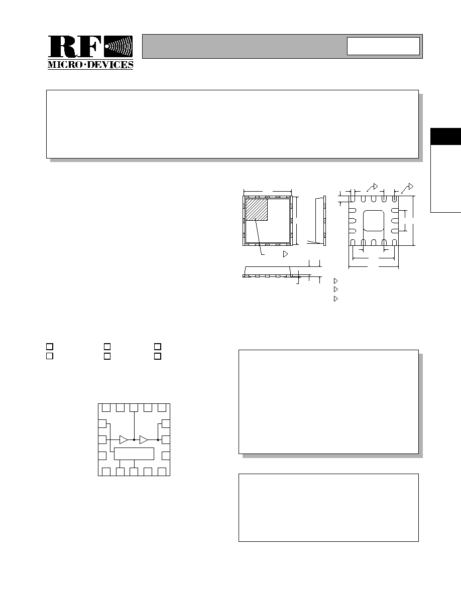
3.75
3.75
+
1.50 SQ
4.00
4.00
1
0.45
0.28
3.20
1.60
0.75
0.50
12∞
INDEX AREA
3
1.00
0.90
0.75
0.65
0.05
0.00
NOTES:
5
Package Warpage: 0.05 max.
4
Pins 1 and 9 are fused.
Shaded Pin is Lead 1.
1
Dimension applies to plated terminal and is measured
0.10 mm and 0.25 mm from terminal tip.
2
The terminal #1 identifier and terminal numbering conv
shall conform to JESD 95-1 SPP-012. Details of termin
identifier are optional, but must be located within the z
indicated. The identifier may be either a mold or marke
feature.
3
0.80
TYP
2
1
Dimensions in mm.
Package Style: LCC, 16-Pin, 4x4

2-214
RF2172
Rev A9 010823
2
PO
W
E
R
A
M
P
LI
FI
E
R
S
Caution! ESD sensitive device.
RF Micro Devices believes the furnished information is correct and accurate
at the time of this printing. However, RF Micro Devices reserves the right to
make changes to its products without notice. RF Micro Devices does not
assume responsibility for the use of the described product(s).
Absolute Maximum Ratings
Parameter
Rating
Unit
Supply Voltage (RF off)
-0.5 to +6.0
V
DC
APC Current (Maximum)
+10
mA
Control Voltage (V
PD
)
-0.5 to +6.0
V
DC
Input RF Power
+10
dBm
Operating Case Temperature
-40 to +85
∞C
Storage Temperature
-55 to +155
∞C
Parameter
Specification
Unit
Condition
Min.
Typ.
Max.
Overall
T = 25∞C, V
CC
= 3.6V, V
PD
= 3.6V, V
APC
= 2.5V
Usable Frequency Range
500 to 2500
MHz
Input Impedance
50
Input VSWR
1.8:1
Without Input Match
Output Load VSWR
<10:1
0< V
APC
<3.0V
<6:1
0<V
APC
<3.6V
2.45GHz Operation
Freq= 2.4GHz to 2.5GHz, P
IN
=0dBm
Operating Frequency
2.4 to 2.5
GHz
Maximum Output Power
22
+23.5
24.5
dBm
Total Efficiency
45
%
Reverse Isolation
-25
dB
Second Harmonic
-45
dBc
Third Harmonic
-40
dBc
All Other Spurious
-50
dBc
Output Load Impedance
20-j4.5
Present to part
Gain Control Voltage
0 to V
CC
V
High Gain
+22
dB
V
APC
= 3.6V, V
CC
= 3.6V, P
IN
=0dBm
Low Gain
-10
dB
V
APC
=0V, V
CC
=3.6V, P
IN
=0dBm
902MHz Operation
Freq= 902MHz to 928MHz, P
IN
=-3.0dBm
Operating Frequency
902 to 928
MHz
Maximum Output Power
+24
dBm
Total Efficiency
58
%
Reverse Isolation
-35
dB
Second Harmonic
-40
dBc
Third Harmonic
-40
dBc
All Other Spurious
-50
dBc
Output Load Impedence
20-j1.6
Present to part
Gain Control Voltage
0 to V
CC
V
Gain Control Slope
20
dB/V
Gain
0 to 28
dB
Power Supply
Power Supply Voltage
3.6
V
Power Supply Current
145
mA
V
CC
=3.6V, V
APC
= 3.6V, P
IN
=-3dBm,
V
PD
=3.6V
Idle Current
35
mA
V
PD
=3.6V, V
APC
= 3.6V, RF P
IN
<-30dBm
Power Down Current
2.8
10
µ
A
V
CC
=3.6V, V
APC
=0V, V
PD
= 0V total I
CC
I(PD)
4.5
mA
V
CC
=3.6V, V
PD
= 3.6V into PD pin
I(PD)
2.25
mA
V
CC
=3.0V, V
PD
= 3.0V into PD pin

2-215
RF2172
Rev A9 010823
2
PO
W
E
R
A
M
P
LI
FI
E
R
S
Pin
Function
Description
Interface Schematic
1
GND
Ground connection. For best performance, keep traces physically short
and connect immediately to the ground plane.
2
GND
Ground connection for the driver stage. For best performance, keep
traces physically short and connect immediately to the ground plane.
3
RF IN
RF input. This is a 50
input. No external matching is needed. An
external DC blocking capacitor is required if this port is connected to a
DC path to ground or a DC voltage.
See pin 15.
4
GND
See pin 1.
5
GND
See pin 1.
6
VPD
Power down pin. When this pin is 0V, the device will be in power down
mode, dissipating minimum DC power. This pin also serves as the V
CC
supply pin for the bias circuitry. V
PD
should be at the supply voltage
when the part is not in power down mode.
7
APC
Analog power control. Output power varies as a function of the voltage
on this pin. See graph. This pin must be driven through a series resistor
with a voltage between 0V and V
CC
. Series resistor determines
dynamic range of power control. See plot "P
OUT
versus Gain Control
versus Gain Control Resistor".
8
GND
See pin 1.
9
GND
See pin 1.
10
GND
See pin 1.
11
RF OUT
RF output. An external matching network is required to provide the opti-
mum load impedance at this pin.
See pin 15.
12
RF OUT
RF output and power supply for the output stage. Bias voltage for the
output stage is provided through this pin. A shunt cap resonating with
the bond wire inductance at 2xf
0
can also be used at this pin to provide
a second harmonic trap.
See pin 15.
13
GND
See pin 1.
14
GND
See pin 1.
15
VCC
Power supply for driver stage and interstage matching. This pin forms
the shunt inductance needed for proper tuning of the interstage. Refer
to the application schematic for the proper configuration. Note: Position
and value of the components are important.
16
GND
See pin 1.
Pkg
Base
GND
Ground connection for the output stage. This pad should be connected
to the groundplane by vias directly under the device. A short path is
required to obtain optimum performance, as well as provide a good
thermal path to the PCB for maximum heat dissipation.
APC
Bias
Network
RF IN
1st
Stage
GND
External Cap
V
CC
Inductor
Bond
Wire
Pin 15
RF OUT
1st Stage
2nd Stage
RF IN
RF OUT

2-216
RF2172
Rev A9 010823
2
PO
W
E
R
A
M
P
LI
FI
E
R
S
Application Schematic - 915MHz
Application Schematic - 2.45GHz
12
11
10
2
4
3
13
14
15
16
1
9
8
7
6
5
22 nF
RF IN
3.9 nH
R
APC
3 k
APC
2.7 nH
22 nF
4 pF
3.9 nH
4 pF
RF OUT
Bias
22 nF
22 nF
22 nF
22 nF
V
PD
V
CC
V
CC
12
11
10
2
4
3
13
14
15
16
1
9
8
7
6
5
22 nF
RF IN
200
VAPC
22 nF
1.5 pF
1.5 nH
RF OUT
Bias
4 pF
22 nF
22 nF
22 nF
V
CC
V
CC
10
22 nF
5 pF
5 pF
10
V
CC
0.5 pF

2-217
RF2172
Rev A9 010823
2
PO
W
E
R
A
M
P
LI
FI
E
R
S
Evaluation Board Schematic - 915MHz
(Download Bill of Materials from www.rfmd.com).
12
11
10
2
4
3
13
14
15
16
1
9
8
7
6
5
C2
22 nF
L1
3.9 nH
R2
3 k
VAPC
C6
22 nF
C5
4 pF
L3
3.9 nH
C7
4 pF
Bias
22 nF
C8
22 nF
C4
22 nF
C3
22 nF
R1*
OPEN
VCC2
VCC3
L2
2.7 nH
50
µ
strip
J2
RF OUT
VCC1
50
µ
strip
J1
RF IN
P1
1
2
3
CON3
P1-1
VCC2
GND
P1-3
VCC3
P2
1
2
3
CON3
P2-1
VAPC
GND
P2-3
VCC1

2-218
RF2172
Rev A9 010823
2
PO
W
E
R
A
M
P
LI
FI
E
R
S
Evaluation Board Schematic - 2.45GHz
12
11
10
2
4
3
13
14
15
16
1
9
8
7
6
5
R2
200
VAPC
C8
22 nF
C7
1.5 pF
L1
1.5 nH
Bias
C10
4 pF
C9
22 nF
C5
22 nF
C4
22 nF
R3
10
C11
22 nF
C6
5 pF
C3
5 pF
R1
10
C1
0.5 pF
VCC2
VCC3
VCC1
C2
22 nF
J1
RF IN
50
µ
strip
J2
RF OUT
50
µ
strip
P1
1
2
3
CON3
P1-1
VCC2
GND
P1-3
VCC3
P2
1
2
3
CON3
P2-1
VAPC
GND
P2-3
VCC1
2172401-

2-219
RF2172
Rev A9 010823
2
PO
W
E
R
A
M
P
LI
FI
E
R
S
Evaluation Board Layout - 915MHz
Board Size 0.80" x 0.85"
Board Thickness 0.031", Board Material FR-4
Evaluation Board Layout - 2.45GHz
Board Size 0.800" x 0.924"
Board Thickness 0.031", Board Material FR-4

2-220
RF2172
Rev A9 010823
2
PO
W
E
R
A
M
P
LI
FI
E
R
S
P
OUT
versus P
IN
V
CC
=3.6V, V
APC
=3.6V, Freq=915MHz
-10.0
-5.0
0.0
5.0
10.0
15.0
20.0
25.0
30.0
-25.0
-20.0
-15.0
-10.0
-5.0
0.0
5.0
P
IN
(dBm)
P
OUT
(dBm)
Pout -40
Pout 25
Pout 85
P
OUT
versus P
IN
V
CC
=3.0V, V
APC
=3.0V, Freq=915MHz
-10.0
-5.0
0.0
5.0
10.0
15.0
20.0
25.0
30.0
-25.0
-20.0
-15.0
-10.0
-5.0
0.0
5.0
P
IN
(dBm)
P
OUT
(dBm)
Pout -40
Pout 25
Pout 85
Efficiency versus P
IN
V
CC
=3.6V, V
APC
=3.6V, Freq=915MHz
0.0
10.0
20.0
30.0
40.0
50.0
60.0
70.0
-25.0
-20.0
-15.0
-10.0
-5.0
0.0
5.0
P
IN
(dBm)
Efficiency
(
%)
Eff (%) -40
Eff (%) 25
Eff (%) 85
ICC versus P
IN
V
CC
=3.6V, V
APC
=3.6V, Freq=915MHz
0.02
0.04
0.06
0.08
0.10
0.12
0.14
0.16
0.18
-25.00
-20.00
-15.00
-10.00
-5.00
0.00
5.00
P
IN
(dBm)
I
CC
(A)
Icc -40
Icc 25
Icc 85
POUT versus V
APC
V
CC
=3.6V, Freq=915MHz, P
IN
=-3dBm
-10.0
-5.0
0.0
5.0
10.0
15.0
20.0
25.0
30.0
0.0
0.3
0.6
0.9
1.2
1.5
1.8
2.1
2.4
2.7
3.0
3.3
3.6
V
APC
(V)
P
OUT
(dBm)
Pout -40
Pout 25
Pout 85
ICC versus V
APC
V
CC
=3.6V, Freq=915MHz, P
IN
=-3dBm
0.02
0.03
0.04
0.05
0.06
0.07
0.08
0.09
0.10
0.11
0.12
0.13
0.14
0.15
0.16
0.00
0.30
0.60
0.90
1.20
1.50
1.80
2.10
2.40
2.70
3.00 3.30
3.60
V
APC
(V)
I
CC
(A)
Icc -40
Icc 25
Icc 85

2-221
RF2172
Rev A9 010823
2
PO
W
E
R
A
M
P
LI
FI
E
R
S
I
APC
versus V
APC
V
CC
=3.6V, V
PD
=3.6V, Freq=915MHz
-0.8
-0.6
-0.4
-0.2
0.0
0.2
0.4
0.6
0.0
0.3
0.6
0.9
1.2
1.5
1.8
2.1
2.4
2.7
3.0
3.3
3.6
V
APC
(V)
I
APC
(mA)
Iapc[mA] -40
Iapc[mA] 25
Iapc[mA] 85
P
OUT
versus Gain Control versus R
APC
V
CC
=3.6V, P
IN
=-3dBm, Freq=915MHz
-10.0
-5.0
0.0
5.0
10.0
15.0
20.0
25.0
30.0
0.0
0.3
0.6
0.9
1.2
1.5
1.8
2.1
2.4
2.7
3.0
3.3
3.6
V
APC
(V)
P
OUT
(dBm)
Rapc (3k)
Rapc (3.5k)
Rapc (4k)
P
OUT
versus P
IN
versus R
APC
V
CC
=3.6V, V
APC
=3.6V, Freq=915MHz
-5.0
0.0
5.0
10.0
15.0
20.0
25.0
30.0
-25.0
-20.0
-15.0
-10.0
-5.0
0.0
5.0
P
IN
(dBm)
P
OUT
(dBm)
Rapc (3k)
Rapc (3.5k)
Rapc (4k)
P
OUT
versus P
IN
V
CC
= V
APC
= 3.6V, Freq = 2.45 GHz
-10.0
-5.0
0.0
5.0
10.0
15.0
20.0
25.0
30.0
-25.0
-20.0
-15.0
-10.0
-5.0
0.0
5.0
P
IN
(dBm)
P
OU
T
(d
Bm)
Pout@-40C
Pout@+25C
Pout@+85C
Efficiency versus P
IN
V
CC
= V
APC
= 3.6 V, Freq = 2.45 GHz
0.0
5.0
10.0
15.0
20.0
25.0
30.0
35.0
40.0
45.0
50.0
-25.0
-20.0
-15.0
-10.0
-5.0
0.0
5.0
P
IN
(dBm)
Effi
ci
e
n
c
y
(
%
)
Eff@-40C
Eff@+25C
Eff@+85C
I
CC
versus P
IN
V
CC
= V
APC
= 3.6 V, Freq = 2.45 GHz
0.00
0.05
0.10
0.15
0.20
0.25
-25.00
-20.00
-15.00
-10.00
-5.00
0.00
5.00
P
IN
(dBm)
I
CC
(A)
Icc@-40C
Icc@+25C
Icc@+85C

2-222
RF2172
Rev A9 010823
2
PO
W
E
R
A
M
P
LI
FI
E
R
S
P
OUT
versus V
APC
V
CC
= 3.6 V, Freq = 2.45 GHz, P
IN
= 0 dBm
-15.0
-10.0
-5.0
0.0
5.0
10.0
15.0
20.0
25.0
0.0
0.4
0.8
1.2
1.6
2.0
2.4
2.8
3.2
3.6
V
APC
(V)
P
OU
T
(d
Bm)
Pout@-40C
Pout@+25C
Pout@+85C
P
OUT
versus V
APC
V
CC
= 3.6 V, Freq = 2.45 GHz, P
IN
= 0 dBm
0.00
0.02
0.04
0.06
0.08
0.10
0.12
0.14
0.16
0.18
0.00
0.40
0.80
1.20
1.60
2.00
2.40
2.80
3.20
3.60
V
APC
(V)
P
OU
T
(d
Bm)
Icc@-40C
Icc@+25C
Icc@+85C
f
0
, 2f
0
over Frequency
V
CC
= V
APC
= 3.6 V, P
IN
= 0 dBm
-60.0
-50.0
-40.0
-30.0
-20.0
-10.0
0.0
10.0
20.0
30.0
2400.0
2420.0
2440.0
2460.0
2480.0
2500.0
Frequency (MHz)
f
0
(dBm)
-60.0
-50.0
-40.0
-30.0
-20.0
-10.0
0.0
2f0
(
dBc)
f0@-40C
f0@+25C
f0@+85C
2f0@-40C
2f0@+25C
2f0@+85C
P
OUT
versus P
IN
V
CC
- V
APC
= 3.0 V, Freq = 2.45 GHz
-10.0
-5.0
0.0
5.0
10.0
15.0
20.0
25.0
-25.0
-20.0
-15.0
-10.0
-5.0
0.0
5.0
P
IN
(dBm)
P
OU
T
(d
Bm)
Pout@-40C
Pout@+25C
Pout@+85C
I
CC
versus P
IN
V
CC
= V
APC
= 3.0 V, Freq = 2.45 GHz
0.00
0.02
0.04
0.06
0.08
0.10
0.12
0.14
0.16
-25.00
-20.00
-15.00
-10.00
-5.00
0.00
5.00
P
IN
(dBm)
I
CC
(A)
Icc@-40C
Icc@+25C
Icc@+85C
Efficiency versus P
IN
V
CC
= V
APC
= 3.0 V, Freq = 2.45 GHz
0.0
5.0
10.0
15.0
20.0
25.0
30.0
35.0
40.0
45.0
50.0
-25.0
-20.0
-15.0
-10.0
-5.0
0.0
5.0
P
IN
(dBm)
Effi
ci
e
n
c
y
(
%
)
Eff@-40C
Eff@+25C
Eff@+85C

2-223
RF2172
Rev A9 010823
2
PO
W
E
R
A
M
P
LI
FI
E
R
S
P
OUT
versus V
APC
V
CC
= 3.0 V, Freq = 2.45 GHz, P
IN
= 0 dBm
-15.0
-10.0
-5.0
0.0
5.0
10.0
15.0
20.0
25.0
0.0
0.5
1.0
1.5
2.0
2.5
3.0
V
APC
(V)
P
OU
T
(d
Bm)
Pout@-40C
Pout@+25C
Pout@+85C
I
CC
versus V
APC
V
CC
= 3.0 V, Freq = 2.45 GHz, P
IN
= 0 dBm
0.00
0.02
0.04
0.06
0.08
0.10
0.12
0.14
0.00
0.50
1.00
1.50
2.00
2.50
3.00
V
APC
(V)
I
CC
(A)
Icc@-40C
Icc@+25C
Icc@+85C
P
OUT
versus P
IN
over R2
V
CC
= V
APC
= 3.6 V, Freq = 2450 MHz
-10.0
-5.0
0.0
5.0
10.0
15.0
20.0
25.0
30.0
-25.0
-20.0
-15.0
-10.0
-5.0
0.0
5.0
P
IN
(dBm)
P
OU
T
(d
Bm)
Pout(100)
Pout(200)
Pout(300)
Pout(400)
I
CC
versus P
IN
over R2
V
CC
= V
APC
= 3.6 V, Freq = 2450 MHz
0.00
0.05
0.10
0.15
0.20
0.25
-25.00
-20.00
-15.00
-10.00
-5.00
0.00
5.00
P
IN
(dBm)
I
CC
(A)
Icc(100)
Icc(200)
Icc(300)
Icc(400)
Efficiency versus P
IN
over R2
V
CC
= V
APC
= 3.6 V, Freq = 2450 MHz
0.0
5.0
10.0
15.0
20.0
25.0
30.0
35.0
40.0
45.0
50.0
-25.0
-20.0
-15.0
-10.0
-5.0
0.0
5.0
P
IN
(dBm)
Effi
ci
e
n
c
y
(
%
)
Eff(100)
Eff(200)
Eff(300)
Eff(400)
I
APC
versus V
APC
over R2
V
CC
= 3.6 V, P
IN
= 0 dBm, Freq = 2450 MHz
-0.004
-0.002
0.000
0.002
0.004
0.006
0.008
0.010
0.012
0.000
0.400
0.800
1.200
1.600
2.000
2.400
2.800
3.200
3.600
V
APC
(V)
I
APC
(A)
Iapc(100)
Iapc(200)
Iapc(300)
Iapc(400)

2-224
RF2172
Rev A9 010823
2
PO
W
E
R
A
M
P
LI
FI
E
R
S