
¸
4-43
4
G
E
N
E
RA
L
P
URPO
SE
A
M
P
L
IF
IE
RS
Product Description
Ordering Information
Typical Applications
Features
Functional Block Diagram
RF Micro Devices, Inc.
7625 Thorndike Road
Greensboro, NC 27409, USA
Tel (336) 664 1233
Fax (336) 664 0454
http://www.rfmd.com
Optimum Technology MatchingÆ Applied
Si BJT
GaAs MESFET
GaAs HBT
Si Bi-CMOS
SiGe HBT
Si CMOS
1
2
3
4
8
7
6
5
RF IN
VCC
GND
GND
PD
RF OUT
GND
GC
RF2302
BROADBAND LINEAR
VARIABLE GAIN AMPLIFIER
∑ CDMA Cellular/PCS and JCDMA Systems
∑ TDMA Cellular/PCS Systems
∑ GSM Systems
∑ Wireless Local Loop Systems
∑ Wideband CDMA Systems
∑ PDC Systems (950MHz and 1450MHz)
The RF2302 is a broadband linear variable gain amplifier
that was designed specifically for digital communications
systems that require linear amplification over a wide gain
control range. It is suitable for use in CDMA or TDMA sys-
tems in the cellular or PCS band, in DAMPS systems,
and in PDC systems. Operating supply voltage ranges
from 3 V to 6V. The device operates over a large fre-
quency band, from 100MHz to 2000MHz, and is tuned to
a specific frequency band with an output bias feed induc-
tor and blocking capacitor. Bias optimization may be
achieved by adjusting the voltage to pin 8 (PD). The IC is
manufactured on an advanced Gallium Arsenide Hetero-
junction Bipolar Transistor (GaAs HBT) process and is
featured in a new standard miniature 8-lead plastic
MSOP package.
∑ 25dB Linear Gain Control range
∑ +14dBm OP1dB at 3.5V (836MHz)
∑ Single 3V to 6V Supply
∑ 14dB Max Gain at 836MHz
∑ 10dB Max Gain at 1900MHz
∑ 4dB Noise Figure at 836MHz
RF2302
Broadband Linear Variable Gain Amplifier
RF2302 PCBA-L
Fully Assembled Evaluation Board 836MHz
RF2302 PCBA-H Fully Assembled Evaluation Board 1.88GHz
4
Rev A8 010410
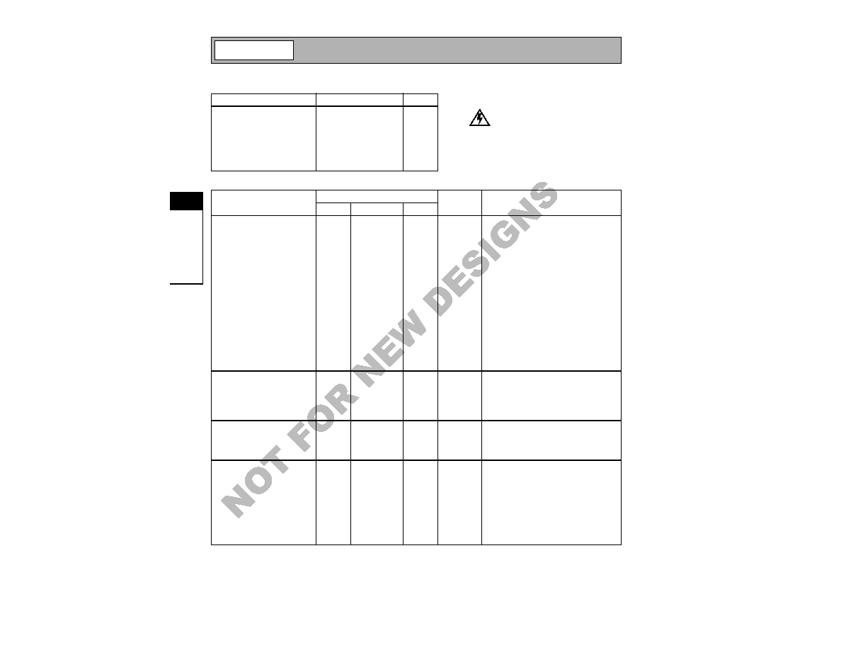
0.006
+ 0.003
0.034
6∞ MAX
0∞ MIN
0.021
+ 0.004
0.006
+ 0.002
NOTES:
1. Shaded lead is pin 1.
2. All dimensions are exclusive of flash,
protrusions or burrs.
3. Lead coplanarity: 0.002 with respect
to datum "A".
A
0.192
+ 0.008
0.0256
0.012
0.118
+ 0.004 sq.
Package Style: MSOP-8
See
Upg
ra
ded
P
rod
uct
RF2
37
6
4-44
RF2302
Rev A8 010410
4
G
E
N
E
RA
L
P
URPO
SE
A
M
P
L
IF
IE
RS
See
Upg
ra
ded
P
rod
uct
RF2
37
6
Absolute Maximum Ratings
Parameter
Rating
Unit
Supply Voltage
0 to +8.0
V
DC
Power Down Voltage
0 to +3.1
V
DC
Gain Control Voltage
0 to +3.1
V
DC
DC Current
100
mA
Output Load VSWR
12:1
Operating Ambient Temperature
-40 to +85
∞C
Storage Temperature
-40 to +150
∞C
Parameter
Specification
Unit
Condition
Min.
Typ.
Max.
Overall
V
CC
= 3.0V, V
PD
= 2.8V, V
GC
=2.2V, T = 25∞C
RF Frequency Range
100
2000
MHz
Small Signal Maximum Gain
13
14
15
dB
Freq= 836MHz, V
GC
=2.2V
9
11
12
dB
Freq= 1880MHz, V
GC
= 2.2V
Small Signal Minimum Gain
-22
-20
-19
dB
Freq= 836MHz, V
GC
=1.4V
-30
-29
-27
dB
Freq= 1880MHz, V
GC
= 1.4V
Noise Figure
4
dB
Freq= 836MHz, V
GC
=2.2V
7
dB
Freq= 1880MHz, V
GC
= 2.2V
Linear Gain Control Range
32
34
dB
V
GC
= 1.4V to 2.2V
Gain Control Slope
1
3
V/V
Slope=
Output peak voltage/
V
GC
Input IP3
+11
+12.5
dBm
Freq=836 MHz, V
GC
= 2.2V
+10
+11
dBm
Freq=1880 MHz, V
GC
=2.2V
-1
+1
dBm
Freq= 836MHz, V
GC
= 1.4V
+1
+3
dBm
Freq= 1880MHz, V
GC
=1.4V
Input VSWR
1.8:1
3:1
In 50
system
Output VSWR
2.5:1
In 50
system
TDMA
ACPR
-33
-34
dBc
836MHz, V
GC
=2.2V
-34
-35
dBc
1880MHz, V
GC
= 2.2V
ALT1
-63
-68
dBc
836MHz, V
GC
=2.2V
-73
-75
dBc
1880MHz, V
GC
= 2.2V
CDMA
ACPR
-50
-52
dBc
836MHz, V
GC
=2.2V
-55
-59
dBc
1880MHz, V
GC
= 2.2V
ALT1
-55
-57
dBc
836MHz, V
GC
=2.2V
Power Supply
T = 25∞C
Supply Voltage
3
6
V
Power Down Voltage High
2.7
2.9
V
Power Down Voltage Low
1.0
DC Current Consumption
40
50
55
mA
V
CC
= 3.0V, V
PD
= 2.8V, V
GC
=1.4V to 2.2V
V
PD
Current
7
9
mA
V
PD
= 2.8V, V
GC
= 2.2V, V
CC
=3.0V
V
GC
Current
16
18
µ
A
V
PD
= 2.8V, V
GC
= 2.2V, V
CC
=3.0V
Power Down Current
10
µ
A
V
PD
<1V, V
GC
<1V
Turn On/Off Time
100
nS
Caution! ESD sensitive device.
RF Micro Devices believes the furnished information is correct and accurate
at the time of this printing. However, RF Micro Devices reserves the right to
make changes to its products without notice. RF Micro Devices does not
assume responsibility for the use of the described product(s).
4-45
RF2302
Rev A8 010410
4
G
E
N
E
RA
L
P
URPO
SE
A
M
P
L
IF
IE
RS
See
Upg
ra
ded
P
rod
uct
RF2
37
6
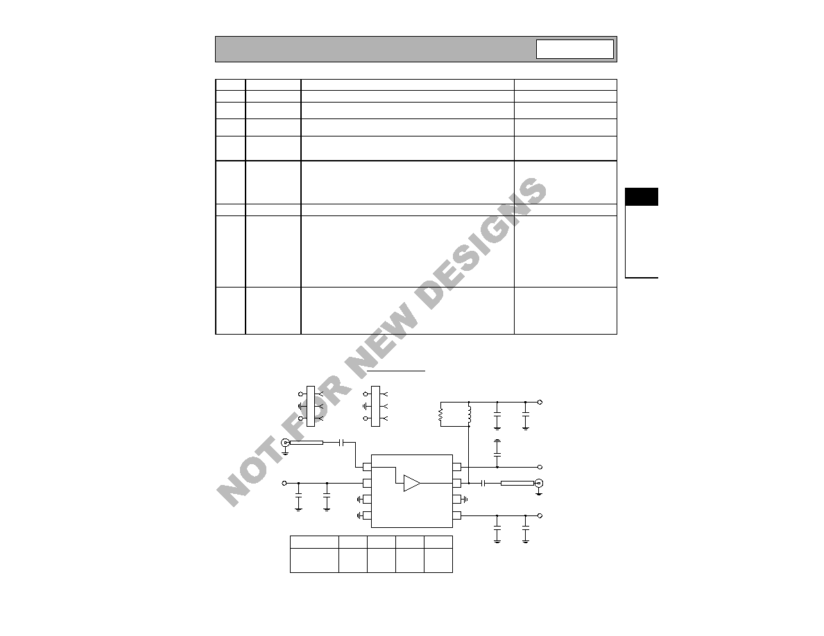
Evaluation Board Schematic - 836MHz or 1900MHz
(Download Bill of Materials from www.rfmd.com.)
Pin
Function
Description
Interface Schematic
1
RF IN
RF input pin. This pin is DC coupled and requires a blocking capacitor.
2
VCC
Power supply. This pin is connected to a battery or a regulated supply
and requires a bypass capacitor as close to the pin as possible.
3
GND
Ground connection. Keep traces physically short and connect immedi-
ately to ground plane for best performance.
4
GND
Ground connection. Keep traces physically short and connect immedi-
ately to ground plane for best performance. Use a separate ground via
for this pin.
5
GC
Analog gain control pin. This pin controls the gain of the IC. Minimum
gain occurs at V
GC
< 1V and maximum gain is achieved with V
GC
= 2.2V.
25dB of linear gain control with no variation of input P
1dB
is available,
and additional attenuation is possible with V
GC
< 1V with input P
1dB
variation. Bypass this pin near the device.
6
GND
Same as pin 3.
7
RF OUT
RF output pin. This pin is DC coupled and requires V
CC
through a bias
inductor sized accordingly to provide a high pass transformation with a
series capacitor. This LC transformation sets the output load line for the
amplifier. If this amplifier is driving a power amplifier or antenna, no
additional matching is required. However, to improve the output match,
a parallel resistor can be added across the inductor. For 836MHz appli-
cations use a 10nH bias inductor (optional resistor R3=100 ohms) and
2.7pF coupling capacitor. For 1900MHz applications use a 2.7nH bias
inductor (optional resistor R3=150ohms) and 1.0pF coupling capacitor.
8
PD
Power down pin. This pin provides bias for the amplifier. To turn the
amplifier on, this pin should be at 2.8V. Reducing this voltage below
0.5V ensures that the amplifier will draw less than 10
µ
A current from
the supply. Additionally, bias current can be optimized for lower output
power by adjusting this voltage over a 2.7V to 2.9V range from a regu-
lated supply.
1
2
3
4
8
7
6
5
L1
C4
C1
22 pF
C11
1nF
C14
1
µ
F
GC
PD
R3
C3
1 nF
C13
1
µ
F
C9
15 pF
C6
C12
1
µ
F
P1-1
P1-3
P1
GND
GC
1
2
3
VCC
P1-1
P1-3
P2
GND
PD
1
2
3
VCC
L (836 MHz)
H (1900 MHz)
Board
R3 (
)
C6 (pF)
C4 (pF)
L1 (nH)
12
3.3
100
150
10
2.7
2.7
1
VCC
50
µ
strip
RF IN
J1
50
µ
strip
RF OUT
J2
VCC
2302400-, 401-
4-46
RF2302
Rev A8 010410
4
G
E
N
E
RA
L
P
URPO
SE
A
M
P
L
IF
IE
RS
See
Upg
ra
ded
P
rod
uct
RF2
37
6
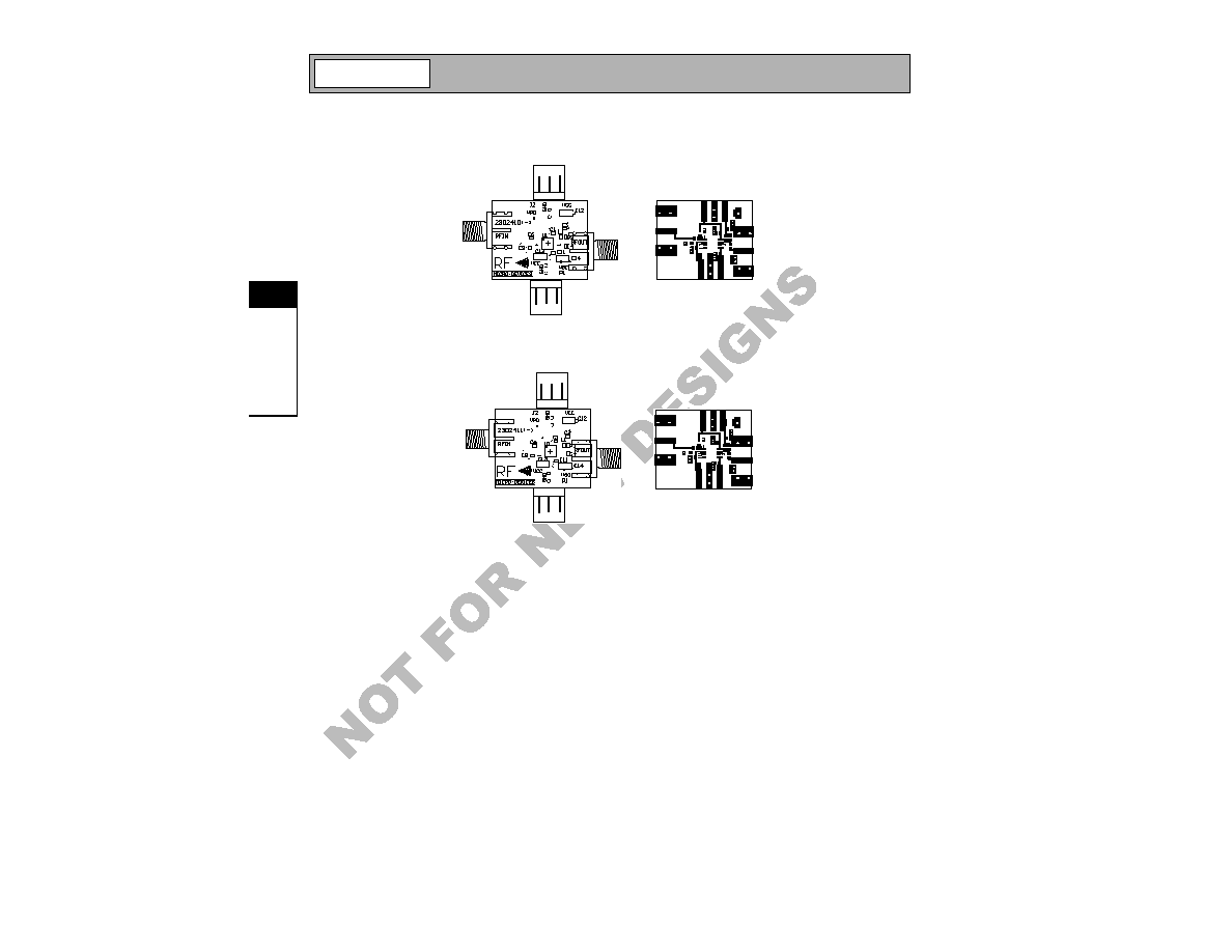
Evaluation Board Layout 836MHz
Board Size 2.0" x 2.0"
Evaluation Board Layout 1.88GHz
4-47
RF2302
Rev A8 010410
4
G
E
N
E
RA
L
P
URPO
SE
A
M
P
L
IF
IE
RS
See
Upg
ra
ded
P
rod
uct
RF2
37
6
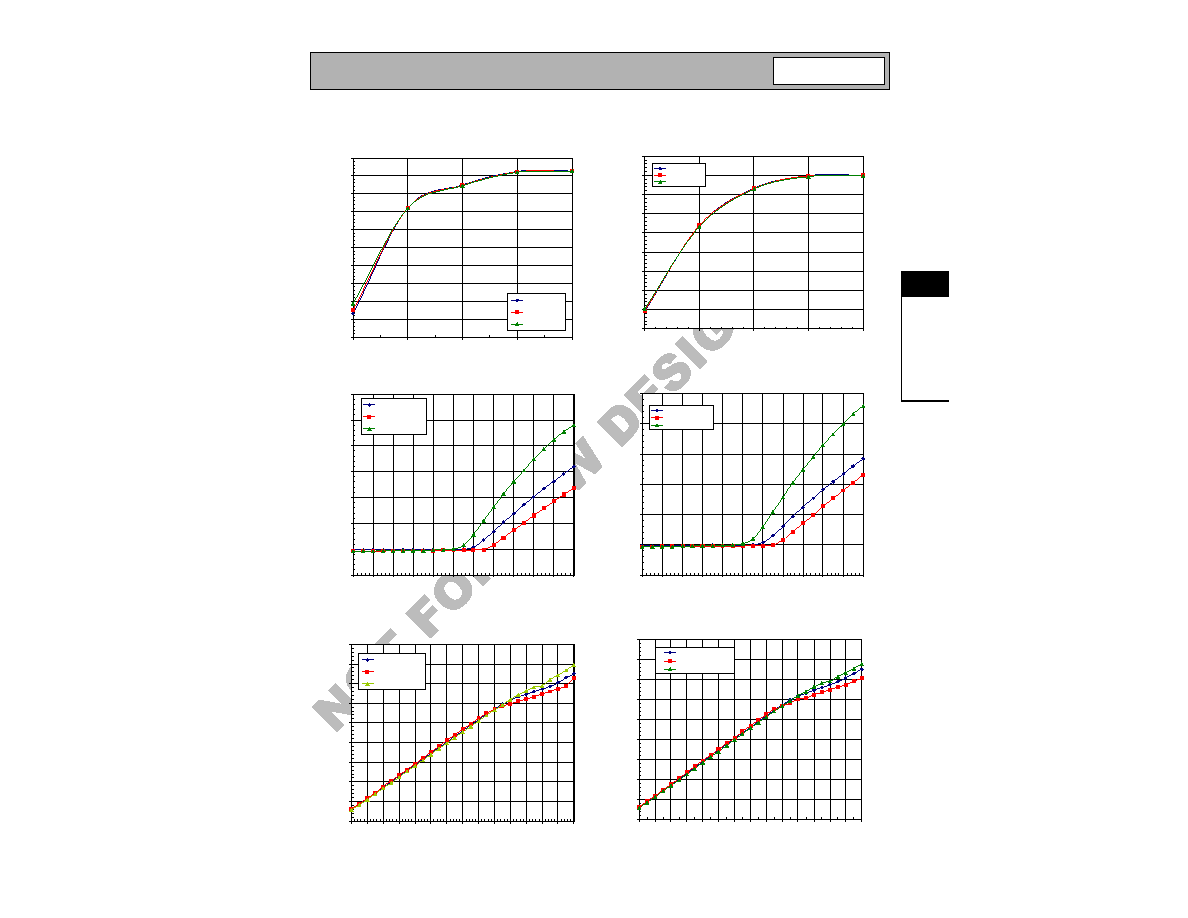
Gain @ 3.3, 3.0, 2.7V versus V
GC
(Frequency 1880MHz @ -8dBm, IS-95 Mod. V
PD
=2.8V,
V
GC
=2.2 to 1.4V)
-35.0
-30.0
-25.0
-20.0
-15.0
-10.0
-5.0
0.0
5.0
10.0
15.0
1.4
1.6
1.8
2.0
2.2
V
GC
(V)
Gain
(dB)
Gain @ 3.3 V
Gain @3.0 V
Gain @ 2.7 v
Gain @ 3.3, 3.0, 2.7V versus V
GC
(Frequency 836MHz @ -6dBm, IS-95 Mod., V
CC
=3.0V, V
PD
=2.8V,
V
GC
=2.2 to 1.4V)
-25.0
-20.0
-15.0
-10.0
-5.0
0.0
5.0
10.0
15.0
20.0
1.4
1.6
1.8
2.0
2.2
V
GC
(V)
Gain
(dB)
Gain @ 3.3 V
Gain @ 3.0 V
Gain @ 2.7 V
I
GC
versus V
GC
(Frequency 1880MHz @ -8dBm, V
CC
=3.0V, V
PD
=2.8V)
-5.0
0.0
5.0
10.0
15.0
20.0
25.0
30.0
0.0
0.2
0.4
0.6
0.8
1.0
1.2
1.4
1.6
1.8
2.0
2.2
V
GC
(V)
I
GC
(uA)
Igc [UA] @25 C
Igc [UA] @ - 40 C
Igc [UA] @ 85 C
I
GC
versus V
GC
(Frequency 836MHz @ -6dBm, V
CC
=3.0V, V
PD
=2.8V)
-5.0
0.0
5.0
10.0
15.0
20.0
25.0
0.0
0.2
0.4
0.6
0.8
1.0
1.2
1.4
1.6
1.8
2.0
2.2
V
GC
(V)
I
GC
(uA)
Igc [UA] @25 C
Igc [UA] @ - 40 C
Igc [UA] @ 85 C
I
PD
versus V
PD
(Frequency 836MHz @ -6 dBm, V
CC
=3.0V, V
GC
=2.2V)
-1.0
0.0
1.0
2.0
3.0
4.0
5.0
6.0
7.0
8.0
0.0
0.2
0.4
0.6
0.8
1.0
1.2
1.4
1.6
1.8
2.0
2.2
2.4
2.6
2.8
V
PD
(V)
I
PD
(mA)
Ipd [mA] @25 C
Ipd [mA] @ - 40 C
Ipd [mA] @ 85 C
I
PD
versus V
PD
(Frequency 1880MHz,V
CC
=3.0V,V
GC
=2.2V)
-1.0
0.0
1.0
2.0
3.0
4.0
5.0
6.0
7.0
8.0
0.0
0.2
0.4
0.6
0.8
1.0
1.2
1.4
1.6
1.8
2.0
2.2
2.4
2.6
2.8
V
PD
(V)
I
PD
(mA)
Ipd [mA] @25 C
Ipd [mA] @ - 40 C
Ipd [mA] @ 85 C
4-48
RF2302
Rev A8 010410
4
G
E
N
E
RA
L
P
URPO
SE
A
M
P
L
IF
IE
RS
See
Upg
ra
ded
P
rod
uct
RF2
37
6
Gain versus V
GC
(Frequency 836MHz @ -6dBm, IS-95 Mod., V
CC
=3.0V, V
PD
=2.8V,
V
GC
=2.2 to 1.0V)
-25.0
-20.0
-15.0
-10.0
-5.0
0.0
5.0
10.0
15.0
20.0
1.0
1.2
1.4
1.6
1.8
2.0
2.2
V
GC
(V)
Gain
(dB)
Gain @ - 40C
Gain @ 25C
Gain @ 85C
Gain versus V
GC
(Frequency 1880MHz @ -8dBm, IS-95 Mod., V
CC
=3.0V, V
PD
=2.8V
-35.0
-30.0
-25.0
-20.0
-15.0
-10.0
-5.0
0.0
5.0
10.0
15.0
1.0
1.2
1.4
1.6
1.8
2.0
2.2
V
GC
(V)
Gain
(dB)
Gain @ - 40C
Gain @ 25C
Gain @ 85C
Gain versus V
GC
(Frequency 836MHz @ -6dBm, NADC. Mod., V
CC
=3.0V,
V
PD
=2.8V)
-25.0
-20.0
-15.0
-10.0
-5.0
0.0
5.0
10.0
15.0
20.0
1.0
1.2
1.4
1.6
1.8
2.0
2.2
V
GC
(V)
Gain
(dB)
Gain @ - 40C
Gain @ 25C
Gain @ 85C
Gain versus V
GC
(Frequency 1880MHz @ -8dBm, NADC Mod. V
CC
=3.0V,
V
PD
=2.8V)
-35.0
-30.0
-25.0
-20.0
-15.0
-10.0
-5.0
0.0
5.0
10.0
15.0
1.0
1.2
1.4
1.6
1.8
2.0
2.2
V
GC
(V)
Gain
(dB)
Gain @ - 40C
Gain @ 25C
Gain @ 85C
ACPR versus V
GC
(Frequency 1880MHz @ -8dBm, IS-95 Mod., V
CC
=3.0V, V
PD
=2.8V
-80.0
-70.0
-60.0
-50.0
-40.0
-30.0
-20.0
-10.0
0.0
1.0
1.2
1.4
1.6
1.8
2.0
2.2
V
GC
(V)
ACPR(dBc)
ACPR @ 25C
ACPR @ - 40C
ACPR @ 85C
ACPR versus V
GC
(Frequency 836MHz @ -6dBm, IS-95 Mod., V
CC
=3.0V, V
PD
=2.8V)
-70.0
-60.0
-50.0
-40.0
-30.0
-20.0
-10.0
0.0
1.0
1.2
1.4
1.6
1.8
2.0
2.2
Vgc(V)
ACPR
(dBc)
ACPR @ 25C
ACPR @ -40C
ACPR @ 85C

4-49
RF2302
Rev A8 010410
4
G
E
N
E
RA
L
P
URPO
SE
A
M
P
L
IF
IE
RS
See
Upg
ra
ded
P
rod
uct
RF2
37
6
ACPR versus V
GC
(Frequency 1880MHz @ -8dBm.NADC Mod., V
CC
=3.0v,
V
PD
=2.8v)
-37.0
-35.0
-33.0
-31.0
-29.0
-27.0
-25.0
-23.0
1.0
1.2
1.4
1.6
1.8
2.0
2.2
V
GC
(V)
ACPR
(dBc)
ACPR @25C
ACPR @-40C
ACPR @85C
Alternate Channel Power versus V
GC
(Frequency 836MHz @ -6dBm, IS-95 Mod., V
CC
=3.0V, V
PD
=2.8V,
V
GC
=2.2 to 1.0V)
-90.0
-80.0
-70.0
-60.0
-50.0
-40.0
-30.0
-20.0
-10.0
0.0
1.0
1.2
1.4
1.6
1.8
2.0
2.2
V
GC
(V)
Alternate
C
hannel
Power
(
dBc)
ALTR.CH.Power @25C
ALTR.CH.Power @-40C
ALTR.CH.Power @85C
Alternate Channel Power versus V
GC
(Frequency 836MHz @ -6dBm, NADC. Mod., V
CC
=3.0V,V
PD
=2.8V,
V
GC
=2.2 to 1.0V)
-90.0
-80.0
-70.0
-60.0
-50.0
-40.0
-30.0
-20.0
-10.0
0.0
1.0
1.2
1.4
1.6
1.8
2.0
2.2
V
GC
(V)
Alternate
C
hannel
Power
(
dBc)
ALTR.Ch.Power @25C
ALTR.Ch.Power @-40C
ALTR.Ch.Power @85C
Alternate Channel Power versus V
GC
.
(Frequency 1880MHz @ -8dBm, IS-95 Mod., V
CC
=3.0V, V
PD
=2.8)
-90.0
-80.0
-70.0
-60.0
-50.0
-40.0
-30.0
-20.0
-10.0
0.0
1.0
1.2
1.4
1.6
1.8
2.0
2.2
V
GC
(V)
Alternate
C
hannel
Power
(
dBc)
ALTR.CH.Power @ 25C
ALTR.CH.Power @ -40C
ALTR.CH.Power @ 85C
Alternate Channel Power versus V
GC
(Frequency 1880MHz @-8dBm, NADC Mod., V
CC
=3.0V,
V
PD
=2.8V)
-80.0
-75.0
-70.0
-65.0
-60.0
-55.0
-50.0
1.0
1.2
1.4
1.6
1.8
2.0
2.2
V
GC
(V)
Alternate
C
hannel
Power
(
dBc)
ALTR.Ch.Power @25C
ALTR.Ch.Power @-40C
ALTR.Ch.Power @85C
ACPR. versus V
GC
(Frequency 836MHz @ -6dBm, NADC.Mod., V
CC
=3.0v, V
PD
=2.8V,
V
GC
=2.2 to 1.0V)
-40.0
-35.0
-30.0
-25.0
-20.0
-15.0
-10.0
-5.0
0.0
1.0
1.2
1.4
1.6
1.8
2.0
2.2
V
GC
(V)
ACPR.
(
dBc)
ACPR @25C
ACPR @-40C
ACPR @85C

4-
5
0
RF230
2
R
e
v
A
8
0104
10
4
GENERAL PURPOSE
AMPLIFIERS
See
Upg
ra
ded
Prod
uct
RF2
37
6