¸
4-63
4
G
E
N
E
RA
L
P
URPO
SE
A
M
P
L
IF
IE
RS
Product Description
Ordering Information
Typical Applications
Features
Functional Block Diagram
RF Micro Devices, Inc.
7625 Thorndike Road
Greensboro, NC 27409, USA
Tel (336) 664 1233
Fax (336) 664 0454
http://www.rfmd.com
Optimum Technology MatchingÆ Applied
Si BJT
GaAs MESFET
GaAs HBT
Si Bi-CMOS
SiGe HBT
Si CMOS
1
2
3
4
8
7
6
5
RF IN
GND
GND
GND
RF OUT
GND
GND
GND
RF2306
GENERAL PURPOSE AMPLIFIER
∑ Broadband, Low Noise Gain Blocks
∑ IF or RF Buffer Amplifiers
∑ Driver Stage for Power Amplifiers
∑ Final PA for Low Power Applications
∑ Portable Battery Powered Equipment
∑ Broadband Test Equipment
The RF2306 is a general purpose, low cost RF amplifier
IC. The device is manufactured on an advanced Gallium
Arsenide Heterojunction Bipolar Transistor (HBT) pro-
cess, and has been designed for use as an easily-cas-
cadable 50
gain block. Applications include IF and RF
amplification in wireless voice and data communication
products operating in frequency bands up to 2000MHz.
The device is self-contained with 50
input and output
impedances and requires only two external DC biasing
elements to operate as specified.
∑ DC to 2000MHz Operation
∑ Internally matched Input and Output
∑ 20dB Small Signal Gain
∑ 3.5dB Noise Figure
∑ 10mW Linear Output Power
∑ Single Positive Power Supply
RF2306
General Purpose Amplifier
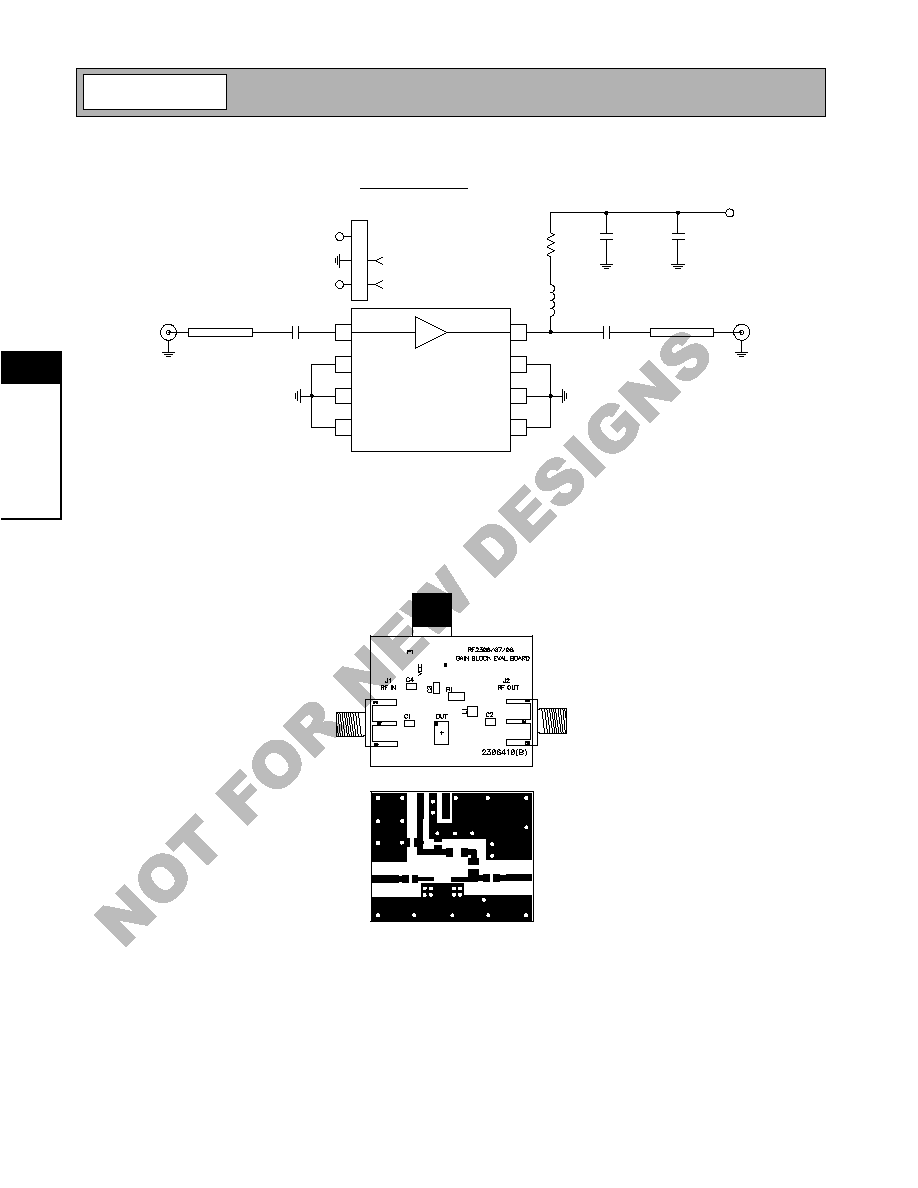
RF2306 PCBA
Fully Assembled Evaluation Board
4
Rev B2 000228
.156
.152
.022
.018
5∞
.056
.052
.195
.191
.240
.232
.050
.008
.004
MIN
.017
1
Package Style: SOP-8

4-64
RF2306
Rev B2 000228
4
G
E
N
E
RA
L
P
URPO
SE
A
M
P
L
IF
IE
RS
Absolute Maximum Ratings
Parameter
Rating
Unit
Supply Current
65
mA
Input RF Power
+10
dBm
Operating Ambient Temperature
-40 to +85
∞C
Storage Temperature
-40 to +150
∞C
Parameter
Specification
Unit
Condition
Min.
Typ.
Max.
Overall
T=25 ∞C, V
CC
= 4.3V, R
C
= 22
,
Freq= 1000MHz
Frequency Range
DC to 2000
MHz
Gain
18
19.5
22
dB
Freq= 1000MHz
19.5
21
23.5
dB
Freq= 100MHz
Noise Figure
3.5
dB
Input VSWR
< 2:1
In a 50
system
Output VSWR
<2:1
In a 50
system
Output IP
3
+20
dBm
Output P
1dB
+10
+12
dBm
Saturated Output Power
+15
dBm
Reverse Isolation
> 20
dB
Power Supply
Operating Voltage
3.7
V
At pin 8
Operating Current
28
35
42
mA
V
CC
= 4.3V, R
C
= 22
Operating Current Range
20 to 65
mA
Caution! ESD sensitive device.
RF Micro Devices believes the furnished information is correct and accurate
at the time of this printing. However, RF Micro Devices reserves the right to
make changes to its products without notice. RF Micro Devices does not
assume responsibility for the use of the described product(s).
4-65
RF2306
Rev B2 000228
4
G
E
N
E
RA
L
P
URPO
SE
A
M
P
L
IF
IE
RS
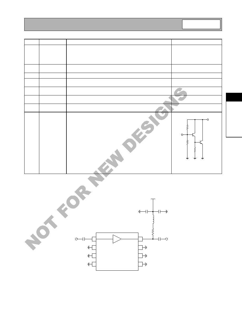
Application Schematic
Pin
Function
Description
Interface Schematic
1
RF IN
RF input pin. This pin is NOT internally DC blocked. A DC blocking
capacitor, suitable for the frequency of operation, should be used in
most applications. DC coupling of the input is not allowed, because this
will override the internal feedback loop and cause temperature instabil-
ity.
2
GND
Ground connection. Keep traces physically short and connect immedi-
ately to ground plane for best performance.
3
GND
Same as pin 2.
4
GND
Same as pin 2.
5
GND
Same as pin 2.
6
GND
Same as pin 2.
7
GND
Same as pin 2.
8
RF OUT
RF output and bias pin. Biasing is accomplished with an external series
resistor and choke inductor to V
CC
. The resistor is selected to set the
DC current into this pin to a desired level. At room temperature, this pin
will bias itself to 3.7V as long as the current is held between 20mA and
65mA. Thus the resistor value is determined by the following equation:
Care should also be taken in the resistor selection to ensure that the
current into the part never exceeds 65 mA over the planned oper-
ating temperature. This means that a resistor between the supply and
this pin is always required, even if a supply near 3.7V is available.
Because DC is present on this pin, a DC blocking capacitor, suitable for
the frequency of operation, should be used in most applications. The
supply side of the bias network should also be well bypassed.
R
V
SUPPL Y
3.7
≠
(
)
I
CC
----------------------------------------
=
RF OUT
RF IN
1
2
3
4
8
7
6
5
RF OUT
22 pF
22
10 nF
22 pF
47 nH
22 pF
RF IN
V
CC
= 4.3V