 | –≠–ª–µ–∫—Ç—Ä–æ–Ω–Ω—ã–π –∫–æ–º–ø–æ–Ω–µ–Ω—Ç: RF2310 | –°–∫–∞—á–∞—Ç—å:  PDF PDF  ZIP ZIP |

¸
4-75
4
G
E
N
E
RA
L
P
URPO
SE
A
M
P
L
IF
IE
RS
Product Description
Ordering Information
Typical Applications
Features
Functional Block Diagram
RF Micro Devices, Inc.
7628 Thorndike Road
Greensboro, NC 27409, USA
Tel (336) 664 1233
Fax (336) 664 0454
http://www.rfmd.com
Optimum Technology MatchingÆ Applied
Si BJT
GaAs MESFET
GaAs HBT
Si Bi-CMOS
SiGe HBT
Si CMOS
1
2
3
4
8
7
6
5
VCC
GND
GND
RF IN
RF OUT
GND
GND
GND
RF2310
WIDEBAND GENERAL PURPOSE AMPLIFIER
∑ General Purpose High Bandwidth Gain
Blocks
∑ IF or RF Buffer Amplifiers
∑ Broadband Test Equipment
∑ Final PA for Medium Power Applications
∑ Driver Stage for Power Amplifiers
The RF2310 is a general purpose, low-cost, high linearity
RF amplifier IC. The device is manufactured on an
advanced Gallium Arsenide Heterojunction Bipolar Tran-
sistor (HBT) process, and has been designed for use as
an easily cascadable 50
gain block. Applications
include IF and RF amplification in wireless voice and data
communication products operating in frequency bands up
to 2500 MHz. The gain flatness over a very wide band-
width makes the device suitable for many applications.
The device is self-contained with 50
input and output
impedances and requires only two external DC biasing
elements to operate as specified.
∑ DC to well over 2500MHz Operation
∑ Internally Matched Input and Output
∑ 15dB Small Signal Gain
∑ 5dB Noise Figure
∑ +19dBm Output Power
∑ Single 3.5V to 6V Positive Power Supply
RF2310
Wideband General Purpose Amplifier
RF2310 PCBA
Fully Assembled Evaluation Board
4
Rev C5 010717
0.244
0.229
0.157
0.150
0.018
0.014
0.050
0.068
0.053
NOTES:
1. Shaded lead is Pin 1.
2. All dimensions are excluding
mold flash.
3. Lead coplanarity -
0.005 with respect to datum "A".
Dimensions in mm
0.196
0.189
0.008
0.004
-A-
8∞ MAX
0∞ MIN
0.034
0.016
0.009
0.007
Package Style: SOIC-8
4-76
RF2310
Rev C5 010717
4
G
E
N
E
RA
L
P
URPO
SE
A
M
P
L
IF
IE
RS
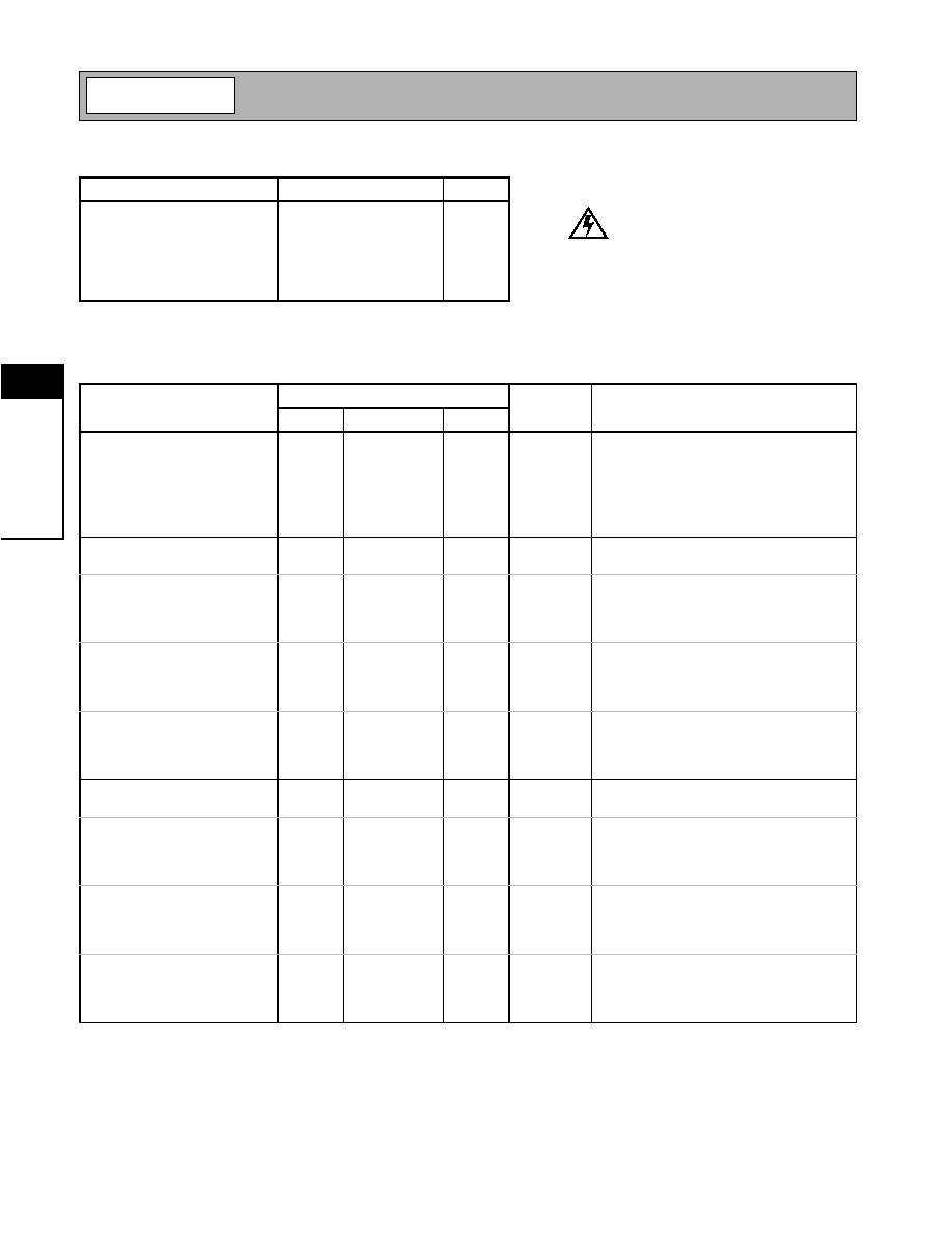
Absolute Maximum Ratings
Parameter
Rating
Unit
Supply Voltage
-0.5 to +6.0
V
DC
Input RF Power
+10
dBm
Storage Temperature
-40 to +150
∞C
Junction Temperature
175
∞C
Thermal Resistance, Junction to
Case
179
∞C/W
Notes: case reference: pins 5-7, conditions: no signal in and both RF ports
terminated in 50
; average junction temperature measured at 85∞C
ambient: 143∞C
Parameter
Specification
Unit
Condition
Min.
Typ.
Max.
Operating Range
Overall Frequency Range
100
2500
MHz
Supply Voltage
3.5
6.0
V
Operating Current (I
CC
)
20
25
mA
V
CC
= 3.6V, Temp= 27∞C
40
50
65
mA
V
CC
=5V, Temp=27∞C
Operating Ambient Temperature
-40
+85
∞C
3.6V Performance
Gain
16.2
dB
Freq= 300MHz, V
CC
= 3.6V, Temp= 27∞C
Gain
15.3
dB
Freq= 900MHz, V
CC
= 3.6V, Temp= 27∞C
Noise Figure
2.5
dB
Output IP3
+22.0
dBm
OP1dB
+10
dBm
Gain
15
dB
Freq= 1950MHz, V
CC
= 3.6V, Temp=27∞C
Noise Figure
2.7
dB
Output IP3
+23.0
dBm
OP1dB
+10
dBm
Gain
16
dB
Freq= 2450MHz, V
CC
= 3.6V, Temp=27∞C
Noise Figure
2.4
dB
Output IP3
+21.0
dBm
OP1dB
+10
dBm
5 V Performance
Gain
17
dB
Freq= 300MHz, V
CC
= 5V, Temp= 27∞C
Gain
14.0
16.5
dB
Freq= 900MHz, V
CC
= 5V, Temp= 27∞C
Noise Figure
3
dB
Output IP3
+28.0
+31.0
dBm
OP1dB
+17
dBm
Gain
15.6
dB
Freq= 1950MHz, V
CC
=5V, Temp=27∞C
Noise Figure
3.5
dB
Output IP3
+33.0
dBm
OP1dB
+18
dBm
Gain
15
dB
Freq= 2450MHz, V
CC
=5V, Temp=27∞C
Noise Figure
2.8
dB
Output IP3
+26.0
dBm
OP1dB
+17
dBm
Caution! ESD sensitive device.
RF Micro Devices believes the furnished information is correct and accurate
at the time of this printing. However, RF Micro Devices reserves the right to
make changes to its products without notice. RF Micro Devices does not
assume responsibility for the use of the described product(s).
4-77
RF2310
Rev C5 010717
4
G
E
N
E
RA
L
P
URPO
SE
A
M
P
L
IF
IE
RS
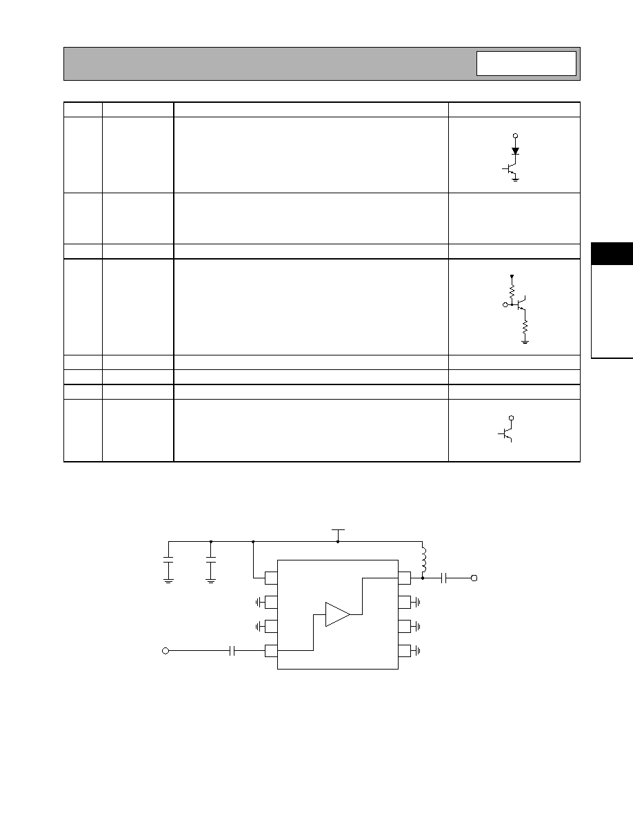
Application Schematic
Pin
Function
Description
Interface Schematic
1
VCC
Power supply pin. An external bypass capacitor is recommended. The
total supply current is shared between this pin and pin 8 (through the
inductor).
2
GND
Ground connection. For best performance, keep traces physically short
and connect immediately to ground plane.
To achieve the performance as specified, and to minimize instability, it
is recommended to have a local ground plane under the device, as
shown in the evaluation board layout.
3
GND
Same as pin 2.
4
RF IN
RF input pin. This pin is NOT internally DC-blocked. A DC-blocking
capacitor, suitable for the frequency of operation, should be used in
most applications. DC-coupling of the input is not allowed, because this
will override the internal feedback loop and cause temperature instabil-
ity.
5
GND
Same as pin 2.
6
GND
Same as pin 2.
7
GND
Same as pin 2.
8
RF OUT
RF output and bias pin. Biasing is accomplished with an external choke
inductor to V
CC
that provides high impedance at the operating fre-
quency. Because DC is present on this pin, a DC-blocking capacitor,
suitable for the frequency of operation, should be used in most applica-
tions. The supply side of the bias network should also be well
bypassed.
VCC
RF IN
Bias
RF OUT
1
2
3
4
8
7
6
5
RF IN
V
CC
= 5V
22 pF
22 pF
100 nH
RF OUT
22 pF
100 nF

4-78
RF2310
Rev C5 010717
4
G
E
N
E
RA
L
P
URPO
SE
A
M
P
L
IF
IE
RS
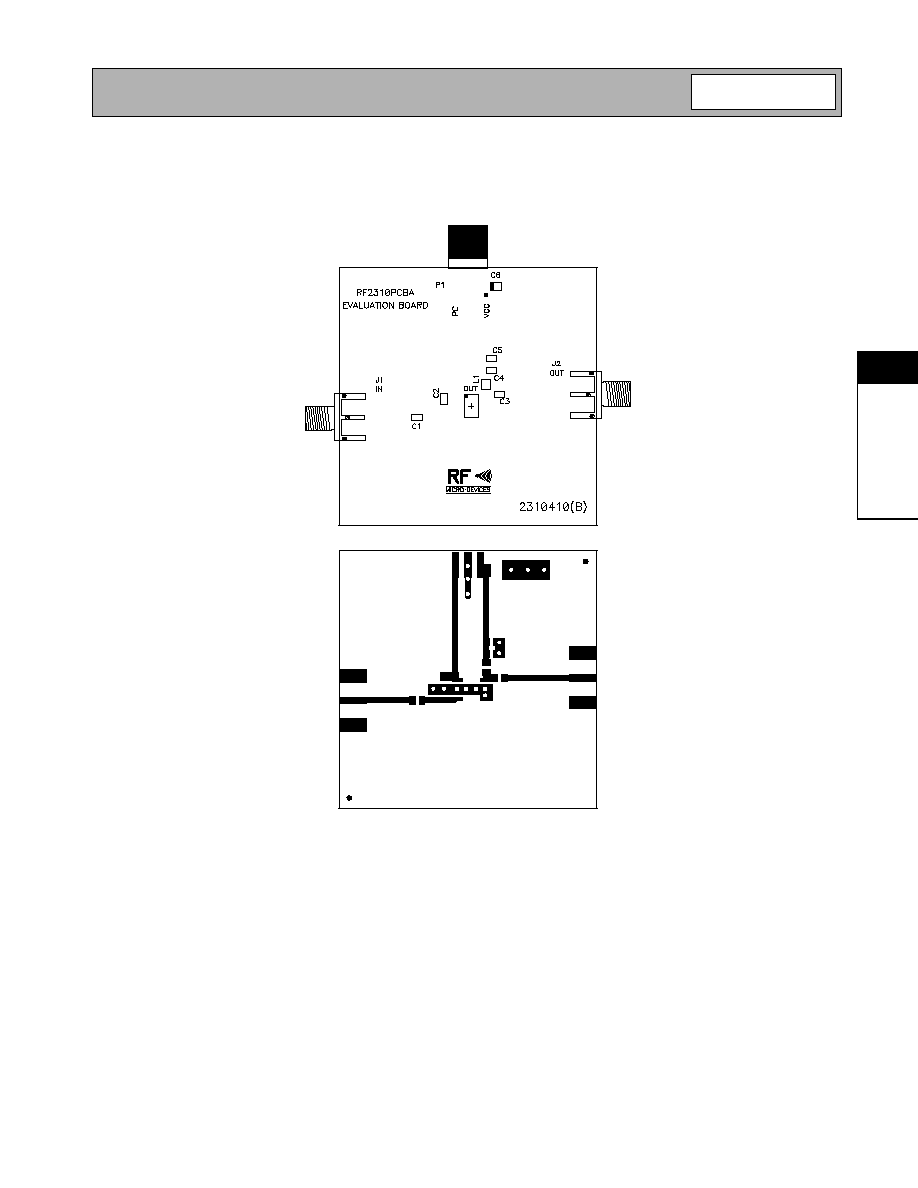
Evaluation Board Schematic
(Download Bill of Materials from www.rfmd.com.)
1
2
3
4
8
7
6
5
P1-3
V
CC
P1-1
V
CC
2310400A
C1
330 pF
50
µ
strip
IN
J1
SMA
C2
1 nF
C3
1 nF
C4
100 pF
50
µ
strip
J2
SMA
OUT
L1
200 nH
C5
330 pF
C6
1
µ
F
P1 H3M
1
2
3
P1-1
PC
GND
P1-3
VCC
4-79
RF2310
Rev C5 010717
4
G
E
N
E
RA
L
P
URPO
SE
A
M
P
L
IF
IE
RS
Evaluation Board Layout
Board Size 2.02" x 2.02"
Board Thickness 0.031", Board Material FR-4

4-80
RF2310
Rev C5 010717
4
G
E
N
E
RA
L
P
URPO
SE
A
M
P
L
IF
IE
RS
S-Parameter Conditions:
All plots are taken at ambient temperature =25∞C.
NOTE:
All S11 and S22 plots shown were taken from an RF2310 evaluation board with external input and output tuning compo-
nents removed and the reference points at the RF IN and RF OUT pins.
0
1.
0
1.
0
-1
.
0
10.
0
10.0
-1
0.0
5.
0
5.0
-5
.0
2.
0
2.
0
-2
.0
3.
0
3.
0
-3
.0
4.
0
4.0
-4
.0
0.
2
0.2
-0.2
0.
4
0.
4
-0
.4
0.
6
0
.6
-0
.6
0.
8
0
.8
-0
.8
S11 Vcc=3V
Swp Max
3.005GHz
Swp Min
0.01GHz
S11 V
CC
= 3V
2.5 GHz
2 GHz
1 GHz
80 MHz
0
1.
0
1.
0
-1
.
0
10.
0
10.0
-1
0.0
5.
0
5.0
-5
.0
2.
0
2.
0
-2
.0
3.
0
3.
0
-3
.0
4.
0
4.0
-4
.0
0.
2
0.2
-0.2
0.
4
0.
4
-0
.4
0.
6
0
.6
-0
.6
0.
8
0
.8
-0
.8
S11 Vcc=5V
Swp Max
3.005GHz
Swp Min
0.01GHz
S11 V
CC
= 5V
1 GHz
2.5 GHz
2 GHz
100 MHz
0
1.
0
1.
0
-1
.
0
10.
0
10.0
-1
0.0
5.
0
5.0
-5
.0
2.
0
2.
0
-2
.0
3.
0
3.
0
-3
.0
4.
0
4.0
-4
.0
0.
2
0.2
-0.2
0.
4
0.
4
-0
.4
0.
6
0
.6
-0
.6
0.
8
0
.8
-0
.8
S22 Vcc=3V
Swp Max
3.005GHz
Swp Min
0.01GHz
S22 V
CC
= 3V
1 GHz
1.6 GHz
2 GHz
100 MHz
0
1.
0
1.
0
-1
.
0
10.
0
10.0
-1
0.0
5.
0
5.0
-5
.0
2.
0
2.
0
-2
.0
3.
0
3.
0
-3
.0
4.
0
4.0
-4
.0
0.
2
0.2
-0.2
0.
4
0.
4
-0
.4
0.
6
0
.6
-0
.6
0.
8
0
.8
-0
.8
S22 Vcc=5V
Swp Max
3.005GHz
Swp Min
0.01GHz
S22 V
CC
= 5V
1 GHz
2 GHz
2.5 GHz
200 MHz
50 MHz

4-81
RF2310
Rev C5 010717
4
G
E
N
E
RA
L
P
URPO
SE
A
M
P
L
IF
IE
RS
Gain versus Temperature
Frequency = 900 MHz
15.4
15.6
15.8
16.0
16.2
16.4
16.6
16.8
17.0
17.2
-60.0
-40.0
-20.0
0.0
20.0
40.0
60.0
80.0
100.0
Temperature (∞C)
Gain
(dB)
Vcc=3V
Vcc=5V
OIP3 versus Temperature
Frequency = 900 MHz
18.0
20.0
22.0
24.0
26.0
28.0
30.0
32.0
34.0
36.0
-60.0
-40.0
-20.0
0.0
20.0
40.0
60.0
80.0
100.0
Temperature (∞C)
OIP3
(dBm)
Vcc=3V
Vcc=5V
OP1dB versus Temperature
Frequency = 900 MHz
5.0
7.0
9.0
11.0
13.0
15.0
17.0
19.0
-60.0
-40.0
-20.0
0.0
20.0
40.0
60.0
80.0
100.0
Temperature (∞C)
OP1dB
(dBm)
Vcc=3V
Vcc=5V
I
CC
versus Temperature
Frequency = 900 MHz
7.0
17.0
27.0
37.0
47.0
57.0
67.0
-60.0
-40.0
-20.0
0.0
20.0
40.0
60.0
80.0
100.0
Temperature (∞C)
I
CC
(mA)
Vcc=3V
Vcc=5V
Gain versus Temperature
Frequency = 1950 MHz
14.6
14.8
15.0
15.2
15.4
15.6
15.8
16.0
16.2
-60.0
-40.0
-20.0
0.0
20.0
40.0
60.0
80.0
100.0
Temperature (∞C)
Gain
(dB)
Vcc=3V
Vcc=5V
OIP3 versus Temperature
Frequency = 1950 MHz
18.0
20.0
22.0
24.0
26.0
28.0
30.0
32.0
34.0
36.0
-60.0
-40.0
-20.0
0.0
20.0
40.0
60.0
80.0
100.0
Temperature (∞C)
OIP3
(dBm)
Vcc=3V
Vcc=5V
4-82
RF2310
Rev C5 010717
4
G
E
N
E
RA
L
P
URPO
SE
A
M
P
L
IF
IE
RS
OP1dB versus Temperature
Frequency = 1950 MHz
5.0
7.0
9.0
11.0
13.0
15.0
17.0
19.0
21.0
-60.0
-40.0
-20.0
0.0
20.0
40.0
60.0
80.0
100.0
Temperature (∞C)
OP1dB
(dBm)
Vcc=3V
Vcc=5V
I
CC
versus Temperature
Frequency = 1950 MHz
8.0
18.0
28.0
38.0
48.0
58.0
68.0
-60.0
-40.0
-20.0
0.0
20.0
40.0
60.0
80.0
100.0
Temperature (∞C)
I
CC
(mA)
Vcc=3V
Vcc=5V
Gain versus Temperature
Frequency = 2450 MHz
12.0
12.5
13.0
13.5
14.0
14.5
15.0
15.5
16.0
-60.0
-40.0
-20.0
0.0
20.0
40.0
60.0
80.0
100.0
Temperature (∞C)
Gain
(dB)
Vcc=3V
Vcc=5V
OIP3 versus Temperature
Frequency = 2450 MHz
17.0
19.0
21.0
23.0
25.0
27.0
29.0
31.0
-60.0
-40.0
-20.0
0.0
20.0
40.0
60.0
80.0
100.0
Temperature (∞C)
OIP3
(dBm)
Vcc=3V
Vcc=5V
OP1dB versus Temperature
Frequency = 2450 MHz
5.0
7.0
9.0
11.0
13.0
15.0
17.0
19.0
-60.0
-40.0
-20.0
0.0
20.0
40.0
60.0
80.0
100.0
Temperature (∞C)
OP1dB
(dBm)
Vcc=3V
Vcc=5V
I
CC
versus Temperature
Frequency = 2450 MHz
7.0
17.0
27.0
37.0
47.0
57.0
67.0
-60.0
-40.0
-20.0
0.0
20.0
40.0
60.0
80.0
100.0
Temperature (∞C)
I
CC
(mA)
Vcc=3V
Vcc=5V

4-83
RF2310
Rev C5 010717
4
G
E
N
E
RA
L
P
URPO
SE
A
M
P
L
IF
IE
RS
S11 of Evaluation Board versus Frequency
Temperature = +25∞C
1.0
1.1
1.2
1.3
1.4
1.5
1.6
1.7
1.8
1.9
0.0
500.0
1000.0
1500.0
2000.0
2500.0
Frequency (MHz)
Input
VSWR
Vcc=3V
Vcc=5V
S22 of Evaluation Board versus Frequency
Temperature = +25∞C
1.0
1.5
2.0
2.5
3.0
3.5
4.0
4.5
5.0
0.0
500.0
1000.0
1500.0
2000.0
2500.0
Frequency (MHz)
Output
VSWR
Vcc=3.0V
Vcc=5.0V
Reverse Isolation (S12) of Evaluation Board versus
Frequency,
Temperature = +25∞C
-24.0
-23.5
-23.0
-22.5
-22.0
-21.5
-21.0
-20.5
-20.0
-19.5
0.0
500.0
1000.0
1500.0
2000.0
2500.0
Frequency (MHz)
Reverse
I
solation
(dB)
Vcc=3.0V
Vcc=5.0V

4-84
RF2310
Rev C5 010717
4
G
E
N
E
RA
L
P
URPO
SE
A
M
P
L
IF
IE
RS