 | –≠–ª–µ–∫—Ç—Ä–æ–Ω–Ω—ã–π –∫–æ–º–ø–æ–Ω–µ–Ω—Ç: RF2317 | –°–∫–∞—á–∞—Ç—å:  PDF PDF  ZIP ZIP |
¸
3-13
3
L
I
NE
A
R
CA
T
V
A
M
P
L
IF
IE
R
S
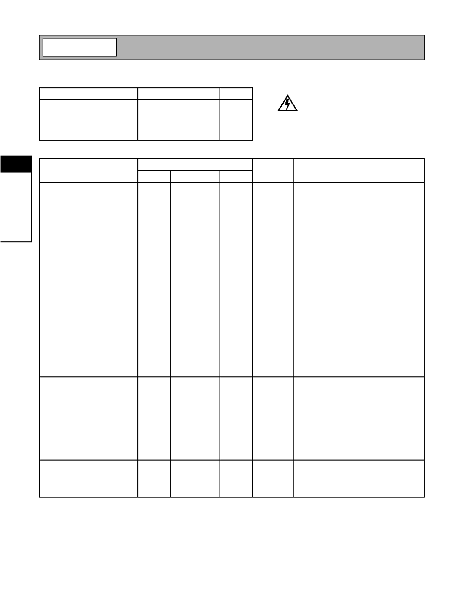
Product Description
Ordering Information
Typical Applications
Features
Functional Block Diagram
RF Micro Devices, Inc.
7625 Thorndike Road
Greensboro, NC 27409, USA
Tel (336) 664 1233
Fax (336) 664 0454
http://www.rfmd.com
Optimum Technology MatchingÆ Applied
Si BJT
GaAs MESFET
GaAs HBT
Si Bi-CMOS
SiGe HBT
Si CMOS
1
2
3
4
5
6
7
8
16
15
14
13
12
11
10
9
NC
GND
GND
RF IN
NC
GND
GND
NC
NC
GND
GND
RF OUT
NC
GND
GND
NC
RF2317
LINEAR CATV AMPLIFIER
∑ CATV Distribution Amplifiers
∑ Cable Modems
∑ Broadband Gain Blocks
∑ Laser Diode Driver
∑ Return Channel Amplifier
∑ Base Stations
The RF2317 is a general purpose, low-cost high-linearity
RF amplifier IC. The device is manufactured on an
advanced Gallium Arsenide Heterojunction Bipolar Tran-
sistor (HBT) process, and has been designed for use as
an easily cascadable 75
gain block. The gain flatness of
better than ±0.5dB from 50MHz to 1000MHz, and the
high linearity, make this part ideal for cable TV applica-
tions. Other applications include IF and RF amplification
in wireless voice and data communication products oper-
ating in frequency bands up to 3GHz. The device is self-
contained with 75
input and output impedances and
requires only two external DC biasing elements to oper-
ate as specified.
∑ DC to 3.0GHz Operation
∑ Internally Matched Input and Output
∑ 15dB Small Signal Gain
∑ 4.9dB Noise Figure
∑ +26dBm Output Power
∑ Single 9V to 12V Power Supply
RF2317
Linear CATV Amplifier
RF2317 PCBA
Fully Assembled Evaluation Board - 50
RF2317 PCBA
Fully Assembled Evaluation Board - 75
3
Rev A16 010816
0.068
0.064
0.020
0.014
0.034 REF
0.068
0.053
0.009
0.007
0.034
0.016
8∞ MAX
0∞ MIN
0.244
0.229
0.393
0.386
0.157
0.150
0.020
REF
0.008
0.004
-A-
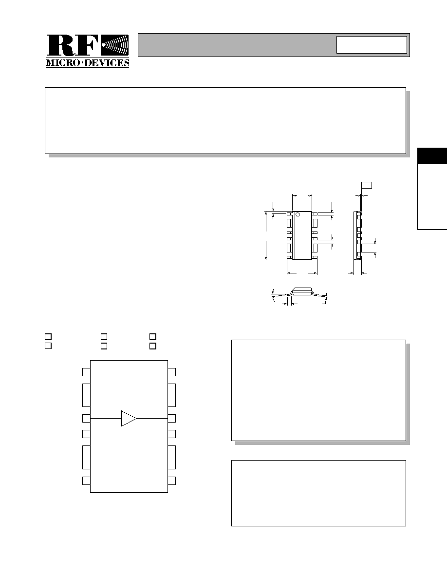
Package Style: CJ2BAT0
3-14
RF2317
Rev A16 010816
3
L
I
NE
A
R
CA
T
V
A
M
P
L
IF
IE
R
S
Absolute Maximum Ratings
Parameter
Rating
Unit
Device Current
250
mA
Input RF Power
+18
dBm
Output Load VSWR
20:1
Ambient Operating Temperature
-40 to +85
∞C
Storage Temperature
-40 to +150
∞C
Parameter
Specification
Unit
Condition
Min.
Typ.
Max.
Overall (50
)
T = 25 ∞C, I
CC
= 180mA, R
C
= 11
, 50
Sys-
tem
Frequency Range
DC
3000
MHz
3dB Bandwidth
Gain
13.5
14.5
15.0
dB
Noise Figure
4.9
dB
From 100MHz to 1000MHz
Input VSWR
1.7
Appropriate values for the DC blocking
capacitors and bias inductor are required to
maintain this VSWR at the intended operat-
ing frequency range.
Output VSWR
2.2
Appropriate values for the DC blocking
capacitors and bias inductor are required to
maintain this VSWR at the intended operat-
ing frequency range.
Output IP
3
+42
dBm
At 100MHz
+37
+40
dBm
At 500MHz
+38
dBm
At 900MHz
Output IP
2
+63
dBm
F
1
= 400MHz, F
2
= 500MHz, F
OUT
= 100MHz
Output P
1dB
+25.5
dBm
At 100MHz
+24
dBm
At 500MHz
+22
dBm
At 900MHz
Saturated Output Power
+26
dBm
At 100MHz
+25
dBm
At 500MHz
+23
dBm
At 900MHz
Reverse Isolation
20
dB
Thermal
Theta
JC
47
∞C/W
I
CC
=150mA, P
DISS
=1.3W, T
AMB
=85∞C
Maximum Junction Temperature
153
∞C
Mean Time Between Failures
8.6x10
2
years
T
AMB
= +85∞C
1.8x10
5
years
T
AMB
= +25∞C
Theta
JC
54
∞C/W
I
CC
=180mA, P
DISS
=1.7W, T
AMB
=85∞C
Maximum Junction Temperature
177
∞C
Mean Time Between Failures
99
years
T
AMB
= +85∞C
9.4x10
3
years
T
AMB
= +25∞C
Power Supply
Device Voltage
8.3
V
On pin 13, I
CC
= 150mA
8.7
V
On pin 13, I
CC
= 180mA
Operating Current Range
100
180
mA
Actual current determined by V
CC
and R
S
Caution! ESD sensitive device.
RF Micro Devices believes the furnished information is correct and accurate
at the time of this printing. However, RF Micro Devices reserves the right to
make changes to its products without notice. RF Micro Devices does not
assume responsibility for the use of the described product(s).
3-15
RF2317
Rev A16 010816
3
L
I
NE
A
R
CA
T
V
A
M
P
L
IF
IE
R
S
Parameter
Specification
Unit
Condition
Min.
Typ.
Max.
Overall (75
)
T= 25∞C, I
CC
= 180mA, R
C
= 11
,
75
System
Frequency Range
DC
3000
MHz
3dB Bandwidth
Gain
15.0
dB
Noise Figure
5.3
dB
From 100MHz to 1000MHz
Input VSWR
1.1:1
Appropriate values for the DC blocking
capacitors and bias inductor are required to
maintain this VSWR at the intended operat-
ing frequency range.
Output VSWR
1.5:1
Appropriate values for the DC blocking
capacitors and bias inductor are required to
maintain this VSWR at the intended operat-
ing frequency range.
Output IP
3
+42
dBm
At 100MHz
+37
+40
dBm
At 500MHz
+38
dBm
At 900MHz
Output IP
2
+63
dBm
F
1
= 400MHz, F
2
= 500MHz, F
OUT
=100MHz
Output P
1dB
+24
dBm
At 100MHz
+23
dBm
At 500MHz
+21
dBm
At 900MHz
Saturated Output Power
+25
dBm
At 100MHz
+24
dBm
At 500MHz
+22
dBm
At 900MHz
Reverse Isolation
20
dB
79 Channels
10dBmV per channel, flat, at the input of the
amplifier; I
CC
=150mA, V
CC
= 10.6V
XMOD
-110
dBc
At 55.25MHz
-78
dBc
At 331.25MHz
-75
dBc
At 547.25MHz
CTB
-88
dBc
At 55.25MHz
-88
dBc
At 331.25MHz
-88
dBc
At 547.25MHz
CSO+1.25MHz
-93
dBc
At 55.25MHz
-78
dBc
At 331.25MHz
-70
dBc
At 547.25MHz
CSO- 1.25MHz
-68
dBc
At 55.25MHz
-78
dBc
At 331.25MHz
-85
dBc
At 547.25MHz
110 Channels
10dBmV per channel, flat, at the input of the
amplifier; I
CC
=150mA, V
CC
= 10.6V
XMOD
-91
dBc
At 55.25MHz
-77
dBc
At 331.25MHz
-75
dBc
At 547.25MHz
CTB
-86
dBc
At 55.25MHz
-85
dBc
At 331.25MHz
-85
dBc
At 547.25MHz
CSO+1.25MHz
-92
dBc
At 55.25MHz
-78
dBc
At 331.25MHz
-71
dBc
At 547.25MHz
CSO- 1.25MHz
-63
dBc
At 55.25MHz
-68
dBc
At 331.25MHz
-81
dBc
At 547.25MHz

3-16
RF2317
Rev A16 010816
3
L
I
NE
A
R
CA
T
V
A
M
P
L
IF
IE
R
S
Pin
Function
Description
Interface Schematic
1
NC
This pin is internally not connected.
2
GND
Ground connection. Keep traces physically short and connect immedi-
ately to ground plane for best performance. Each ground pin should
have a via to the ground plane.
3
GND
Same as pin 2.
4
RF IN
RF input pin. This pin is NOT internally DC blocked. A DC blocking
capacitor, suitable for the frequency of operation, should be used in
most applications. DC coupling of the input is not allowed, because this
will override the internal feedback loop and cause temperature instabil-
ity.
5
NC
This pin is internally not connected.
6
GND
Same as pin 2.
7
GND
Same as pin 2.
8
NC
This pin is internally not connected.
9
NC
This pin is internally not connected.
10
GND
Same as pin 2.
11
GND
Same as pin 2.
12
NC
This pin is internally not connected.
13
RF OUT
RF output and bias pin. Because DC is present on this pin, a DC block-
ing capacitor, suitable for the frequency of operation, should be used in
most applications. For biasing, an RF choke in series with a resistor is
needed. The DC voltage on this pin is typically 8.3V with a current of
150mA. See device voltage versus device current plot. In lower power
applications the value of R
C
can be increased to lower the current and
V
D
on this pin.
14
GND
Same as pin 2.
15
GND
Same as pin 2.
16
NC
This pin is internally not connected.
RF OUT
RF IN
3-17
RF2317
Rev A16 010816
3
L
I
NE
A
R
CA
T
V
A
M
P
L
IF
IE
R
S
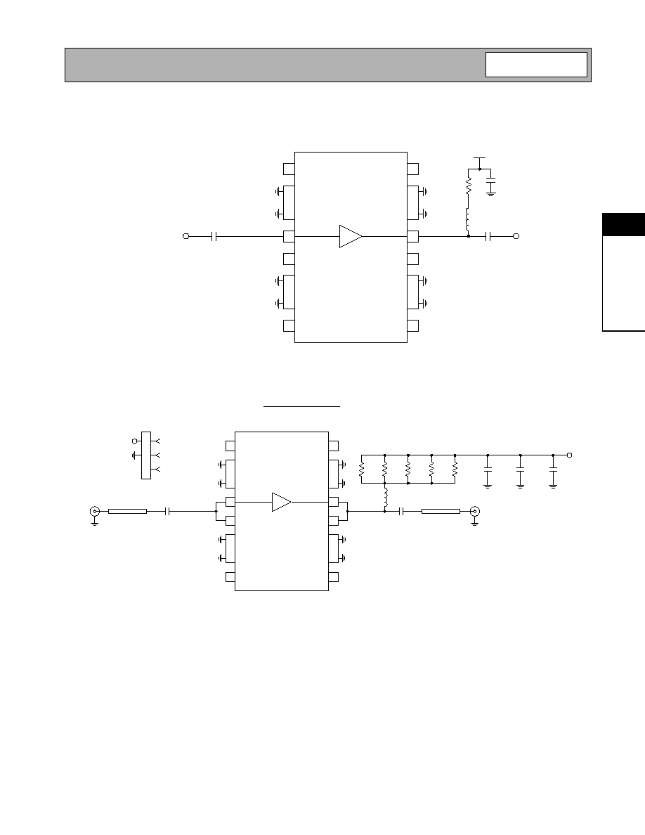
Application Schematic
5MHz to 50MHz Reverse Path
Evaluation Board Schematic - 50
(Download Bill of Materials from www.rfmd.com.)
RF OUT
39
µ
H
11
10 nF
V
CC
1
2
3
4
5
6
7
8
16
15
14
13
12
11
10
9
18 nF
RF IN
18 nF
NOTES:
Gain Flatness <0.5 dB
Input and Output Return Loss >20 dB in 75
system
C1
1 nF
J1
RF IN
C2
1 nF
J2
RF OUT
L1
3.3
µ
H
R1
51
C3
220 pF
R2
51
R3
51
R4
51
VCC
2317400 Rev -
1
2
3
4
5
6
7
8
16
15
14
13
12
11
10
9
C4
100 nF
C5
1
µ
F
R5
51
RT = 10.2
50
µ
strip
50
µ
strip
GND
NC
P1-1
VCC
P1
1
2
3

3-18
RF2317
Rev A16 010816
3
L
I
NE
A
R
CA
T
V
A
M
P
L
IF
IE
R
S
Evaluation Board Schematic - 75
C1
1 nF
J1
RF IN
C2
1 nF
J2
RF OUT
L1
1000 n
H
R4
56
C3
0.1 uF
R1
56
R2
56
R3
56
2317401 Rev -
75
µ
strip
75
µ
strip
GND
NC
P1-1
VCC
P1
1
2
3
VCC
1
3
2
4
6
5
8
7
16
14
15
13
11
12
9
10
3-19
RF2317
Rev A16 010816
3
L
I
NE
A
R
CA
T
V
A
M
P
L
IF
IE
R
S
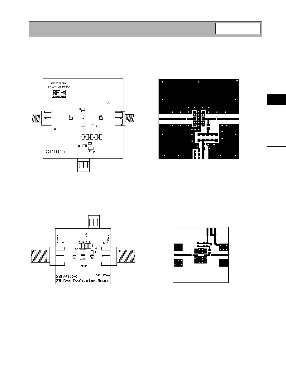
Evaluation Board Layout - 50
2.0" x 2.0"
Board Thickness 0.031", Board Material FR-4
Evaluation Board Layout - 75
1.40" x 1.40"
Board Thickness 0.062", Board Material FR-4

3-20
RF2317
Rev A16 010816
3
L
I
NE
A
R
CA
T
V
A
M
P
L
IF
IE
R
S
Collector Voltage versus Current
4.0
5.0
6.0
7.0
8.0
9.0
10.0
0.0
50.0
100.0
150.0
200.0
250.0
Collector Current (mA)
Collector
Voltage
(Volts)
Vcc
0
1.0
1.0
-1.0
10.0
10.0
-1
0.
0
5.0
5.
0
-5
.0
2.0
2
.
0
-
2
.
0
3.0
3.
0
-3
.0
4.0
4.
0
-4
.0
0.2
0.
2
-0
.2
0.4
0
.
4
-
0
.
4
0.6
0
.
6
-
0
.
6
0.8
0
.
8
-
0
.
8
75 Ohms, ICC = 150 mA, Temp = 25∞C
Swp Max
2GHz
Swp Min
0.005GHz
S[2,2]
S[1,1]
0
1.0
1.0
-1.0
10.0
10.0
-1
0.
0
5.0
5.
0
-5
.0
2.0
2
.
0
-
2
.
0
3.0
3.
0
-3
.0
4.0
4.
0
-4
.0
0.2
0.
2
-0
.2
0.4
0
.
4
-
0
.
4
0.6
0
.
6
-
0
.
6
0.8
0
.
8
-
0
.
8
75 Ohms, ICC = 180 mA, Temp = 25∞C
Swp Max
2GHz
Swp Min
0.005GHz
S[2,2]
S[1,1]
Gain versus Frequency
14.0
14.2
14.4
14.6
14.8
15.0
15.2
15.4
100.0
200.0
300.0
400.0
500.0
Frequency (MHz)
Gain
(dB)
-40 degrees C
+26 degrees C
+85 degrees C