
4-163
4
GEN
E
RA
L
P
URPO
SE
A
M
P
L
IF
IE
RS
�
�
�
�
��
�
RF Micro Devices, Inc.
7625 Thorndike Road
Greensboro, NC 27409, USA
Tel (336) 664 1233
Fax (336) 664 0454
http://www.rfmd.com
��
Si BJT
GaAs MESFET
GaAs HBT
Si Bi-CMOS
SiGe HBT
Si CMOS
1
2
3
4
8
7
6
5
PD
NC
RF IN
GND1
GND2
RF OUT
GND2
GND2
RF2347
�
�
� TDMA/CDMA/FM Cellular LNA
� Low Noise Transmit Driver Amplifier
� General Purpose Amplification
� Commercial and Consumer Systems
The RF2347 is a low noise amplifier with a very high
dynamic range designed for digital cellular applications at
900MHz. The device functions as an outstanding front
end low noise amplifier or power amplifier driver amplifier
in the transmit chain of digital subscriber units where low
transmit noise power is a concern. When used as an
LNA, the bias current can be set externally. When used
as a PA driver, the IC can operate directly from a single
cell Li-ion battery and includes a power down feature that
can be used to completely turn off the device. The IC is
featured in a standard miniature 8-lead plastic MSOP
package.
� Low Noise and High Intercept Point
� Power Down Control
� Single 2.5V to 6.0V Power Supply
� 150MHz to 2500MHz Operation
� Extremely Small MSOP-8 Package
RF2347
3V Low Noise Amplifier/ 3V PA Driver Amplifier
RF2347 PCBA
Fully Assembled Evaluation Board
Rev A5 991207
.026
.120
.116
10�MAX
0�MIN
.009
.005
.120
.116
.196
.190
1
.016
.010
.036
.032
.006
.002
.027
.017
!

4-164
RF2347
Rev A5 991207
4
GEN
E
RA
L
P
URPO
SE
A
M
P
L
IF
IE
RS
Absolute Maximum Ratings
Parameter
Rating
Unit
Supply Voltage
-0.5 to +8.0
V
DC
Input RF Level
+10
dBm
Operating Ambient Temperature
-40 to +85
�C
Storage Temperature
-40 to +150
�C
Parameter
Specification
Unit
Condition
Min.
Typ.
Max.
Overall
RF Frequency Range
150 to 2500
MHz
Low Noise Amplifier
880MHz Performance
Schematic per LNA Application; T = 25�C,
RF=880MHz
Gain
19.5
21.0
dB
V
CC
=3.0V, I
CC
=11mA
19.5
21.0
dB
V
CC
=2.7V, I
CC
=11mA
Noise Figure
1.4
1.6
dB
V
CC
=3.0V, I
CC
=11mA
1.4
1.6
dB
V
CC
=2.7V, I
CC
=11mA
Input IP3
+6.0
dBm
V
CC
=3.0V, I
CC
=11mA
+5.0
dBm
V
CC
=2.7V, I
CC
=11mA
Max Input IP3
+7.5
dBm
V
CC
=3.0V, I
CC
=20mA
+6.0
dBm
V
CC
=2.7V, I
CC
=20mA
Driver Amplifier
836MHz Performance
Schematic per Driver Amplifier Application
T = 25�C, RF=836MHz, V
PD
=2.8V
Gain
19.5
20.5
21.5
dB
V
CC
=3.5V
19.5
20.5
21.5
dB
V
CC
=3.0V
19.5
20.5
21.5
dB
V
CC
=2.5V
Output IP3
25
+28.5
35
dBm
V
CC
=3.5V
+28.5
dBm
V
CC
=3.0V
+27
dBm
V
CC
=2.5V
Noise Figure
1.4
2.0
dB
V
CC
=3.5V
1.4
2.0
dB
V
CC
=3.0V
1.3
2.0
dB
V
CC
=2.5V
Reverse Isolation
26
dB
V
CC
=3.5V
26
dB
V
CC
=3.0V
25
dB
V
CC
=2.5V
Input VSWR
1.5:1
2.0:1
Output VSWR
1.25:1
2.0:1
Using External LC network used on Evalua-
tion Board
P
1dB
13
15.5
dBm
V
CC
=3.5V
12
14.5
dBm
V
CC
=3.0V
10.5
13
dBm
V
CC
=2.5V
Power Supply
T = 25 �C
Voltage (V
CC
)
2.5 to 6.0
V
Voltage (V
PD
)
2.7
2.8
2.9
V
Current Consumption
12.5
22
26.5
mA
V
CC
=3.5V; V
PD
=2.8 V; V
PD
+ V
CC
- Current
Consumption from V
PD
is 2.0 mA Typ. @
V
PD
= 2.8V and 3.0 mA Max @ V
PD
=2.9 V
18
20
22
mA
V
CC
=3.5V; V
PD
=2.7V; V
PD
+ V
CC
19
24
29
mA
V
CC
=3.5V; V
PD
=2.9V; V
PD
+ V
CC
Power Down
10
�
V
CC
=3.5V; V
PD
0.9 V
Caution! ESD sensitive device.
RF Micro Devices believes the furnished information is correct and accurate
at the time of this printing. However, RF Micro Devices reserves the right to
make changes to its products without notice. RF Micro Devices does not
assume responsibility for the use of the described product(s).

4-165
RF2347
Rev A5 991207
4
GEN
E
RA
L
P
URPO
SE
A
M
P
L
IF
IE
RS
Pin
Function
Description
Interface Schematic
1
PD
For low noise amplifier applications, this pin is used to control the bias
current. See plots for bias current settings.
For driver amplifier applications, this is the Power Down pin for the IC.
V
PD
=2.8V +/- 0.1V is required for proper operation. V
PD
< 0.9V turns
off the Part. External RF bypassing is required. The trace length
between the pin and the bypass capacitors should be minimized. The
ground side of the bypass capacitors should connect immediately to
ground plane. Nominal current required for V
PD
=2.8 V is 2.0mA typical
and 3.0mA Max (@ V
PD
=2.9V).
2
NC
No connection. This pin is typically left unconnected or grounded.
3
RF IN
RF input pin. This pin is DC coupled and matched to 50
at 836 MHz.
4
GND1
Ground connection. Keep traces physically short and connect immedi-
ately to ground plane for best performance.
5
NC
See pin 2. This pin is typically grounded.
6
GND2
Ground connection. Keep traces physically short and connect immedi-
ately to ground plane for best performance.
7
RF OUT
Amplifier Output pin. This pin is an open-collector output. It must be
biased to either V
CC
or pin 7 through a choke or matching inductor.
This pin is typically matched to 50
with a shunt bias/matching induc-
tor and series blocking/matching capacitor. Refer to application sche-
matics.
8
GND2
See pin 6.
PD
RF
IN
To Bias
Circuit
RF OUT

4-166
RF2347
Rev A5 991207
4
GEN
E
RA
L
P
URPO
SE
A
M
P
L
IF
IE
RS
�
�
1
2
3
4
8
7
6
5
100 pF
22 nF
VCC
NC
R1
1 k
RF IN
10 nF
VPD
12 nH
100 pF
10 nF
2 pF
RF OUT
1
2
3
4
8
7
6
5
100 pF
22 nF
VCC
NC
R1
0 k
RF IN
10 nF
VPD
12 nH
100 pF
10 nF
2 pF
RF OUT

4-167
RF2347
Rev A5 991207
4
GEN
E
RA
L
P
URPO
SE
A
M
P
L
IF
IE
RS
!"
#$�
(Download Bill of Materials from www.rfmd.com.)
!"
#$�
1
2
3
4
8
7
6
5
50
�strip
C3
22 pF
J1
RF IN
C1
100
pF
C2
10
nF
C4
2 pF
L1
12 nH
50
�strip
J2
RF OUT
C5
100 pF
C6
10 nF
2347400A
PD
VCC
P1-1
VPD
GND
P1-3
C7
4.7
�F
VCC
P1
1
2
3
R1
0
1
2
3
4
8
7
6
5
50
�strip
C3
22 pF
J1
RF IN
C1
100 pF
C2
10 nF
C4
2 pF
L1
12 nH
50
�strip
J2
RF OUT
C5
100 pF
C6
10 nF
2347401-
PD
VCC
P1-1
VPD
GND
P1-3
C7
4.7
�F
VCC
P1
1
2
3
R1
1 k

4-168
RF2347
Rev A5 991207
4
GEN
E
RA
L
P
URPO
SE
A
M
P
L
IF
IE
RS
!"
#$%"
#$�&'()&'(
Board Thickness 0.031"; Board Material FR-4
4-169
RF2347
Rev A5 991207
4
GEN
E
RA
L
P
URPO
SE
A
M
P
L
IF
IE
RS
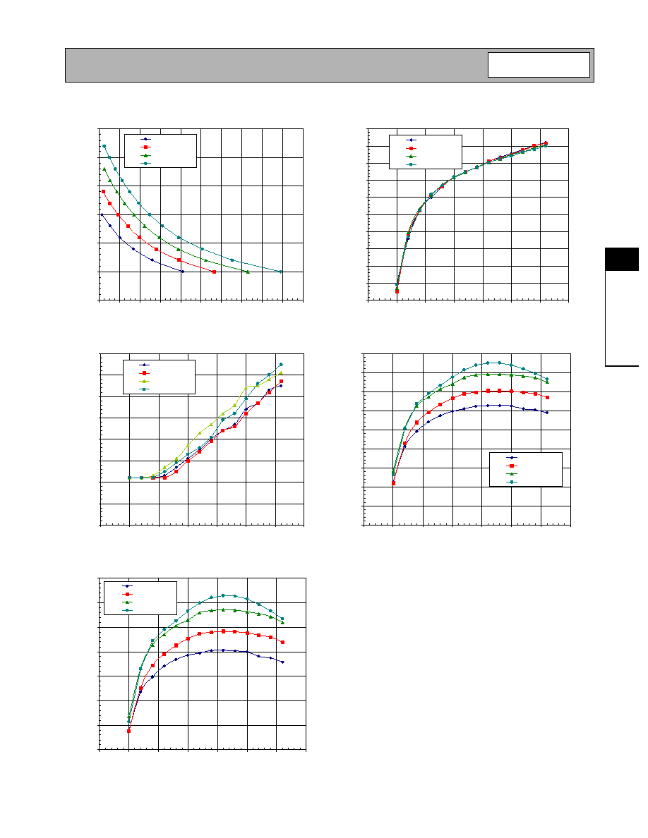
RF2347 Bias Current versus Rc
0
5
10
15
20
25
30
0
200
400
600
800
1000
1200
1400
1600
1800
2000
Rs (
)
Bias Current (mA)
Vcc = 2.7 V
Vcc = 3.0 V
Vcc = 3.3 V
Vcc = 3.6 V
RF2347 Gain versus Bias Current
19.8
20.0
20.2
20.4
20.6
20.8
21.0
21.2
21.4
21.6
21.8
0.0
5.0
10.0
15.0
20.0
25.0
30.0
35.0
Bias Current (mA)
Gain (dB)
Vcc = 2.7 V
Vcc = 3.0 V
Vcc = 3.3 V
Vcc = 3.6 V
RF2347 Noise Figure versus Bias Current
1.2
1.3
1.4
1.5
1.6
1.7
1.8
1.9
2.0
0.0
5.0
10.0
15.0
20.0
25.0
30.0
35.0
Bias Current (mA)
Noise Figure (dB)
Vcc = 2.7 V
Vcc = 3.0 V
Vcc = 3.3 V
Vcc = 3.6 V
RF2347 OIP3 versus Bias Current
15
17
19
21
23
25
27
29
31
33
0
5
10
15
20
25
30
35
Bias Current (mA)
OIP3 (dBm)
2.7V OIP3
3.0V OIP3
3.3V OIP3
3.6V OIP3
RF2347 IIP3 versus Bias Current
-2
0
2
4
6
8
10
12
0
5
10
15
20
25
30
35
Bias Current (mA)
IIP3 (dBm)
Vcc=2.7V
Vcc=3.0 V
Vcc=3.3 V
Vcc=3.6 V

4-170
RF2347
Rev A5 991207
4
GEN
E
RA
L
P
URPO
SE
A
M
P
L
IF
IE
RS