
3-37
3
L
I
NE
A
R
CA
T
V
A
M
P
L
IF
IE
R
S
Preliminary
Product Description
Ordering Information
Typical Applications
Features
Functional Block Diagram
RF Micro Devices, Inc.
7625 Thorndike Road
Greensboro, NC 27409, USA
Tel (336) 664 1233
Fax (336) 664 0454
http://www.rfmd.com
Optimum Technology Matching� Applied
Si BJT
GaAs MESFET
GaAs HBT
Si Bi-CMOS
�
SiGe HBT
Si CMOS
1
2
3
4
5
6
7
8
16
15
14
13
12
11
10
9
NC
NC
GND
GND
GND
RF IN
NC
NC
NC
NC
RF OUT
GND
GND
NC
NC
NC
RF2360
LINEAR GENERAL PURPOSE AMPLIFIER
� CATV Distribution Amplifiers
� Cable Modems
� Broadband Gain Blocks
� Laser Diode Driver
� Return Channel Amplifier
� Base Stations
The RF2360 is a general purpose, low-cost, high-linearity
RF amplifier IC. The device is manufactured on a Gallium
Arsenide process and is featured in an SOP-16 batwing
package. It has been designed for use as an easily cas-
cadable 75
gain block with a Noise Figure of less than
2dB. Gain flatness better than 0.5dB from 5MHz to
1000 MHz, and high linearity make this part ideal for cable
TV applications. Other applications include IF and RF
amplification in wireless voice and data communication
products operating in frequency bands up to 1000MHz.
The device is self-contained with 75
input and output
impedances providing less than 2:1 VSWR matching. For
higher input and output return losses, see the evaluation
schematic.
� 5MHz to 1500MHz Operation
� Internally Matched Input and Output
� 20dB Small Signal Gain
� 1.2dB Noise Figure
� +24dBm Output Power
� Single 6V to 9V Positive Power Supply
RF2360
Linear General Purpose Amplifier
RF2360 PCBA
Fully Assembled Evaluation Board 50
RF2360 411
Fully Assembled Evaluation Board 75H
RF2360 412
Fully Assembled Evaluation Board 75L
3
Rev A9 010824
0.035
0.016
0.010
0.008
8� MAX
0� MIN
0.021
0.014
0.392
0.386
0.158
0.150
0.244
0.230
0.069
0.064
0.050
0.060
0.054
-A-
0.009
0.004
Package Style: Standard Batwing

Preliminary
3-38
RF2360
Rev A9 010824
3
L
I
NE
A
R
CA
T
V
A
M
P
L
IF
IE
R
S
Absolute Maximum Ratings
Parameter
Rating
Unit
Device Current
175
mA
Device Voltage
9
V
Input RF Power
+13
dBm
Output Load VSWR
20:1
Ambient Operating Temperature
-40 to +85
�C
Storage Temperature
-40 to +150
�C
Parameter
Specification
Unit
Condition
Min.
Typ.
Max.
Overall (50
)
T = 25 �C, V
DD
= 7V, 50
System,
P
IN
=-8dBm
Frequency Range
5
1500
MHz
3dB Bandwidth
Input VSWR
1.6:1
Appropriate values for the output DC block-
ing capacitor and bias inductor are required
to maintain this VSWR over the intended
operating frequency range.
Output VSWR
1.2:1
See note for Input VSWR.
Gain
20
dB
At 500MHz
Gain Flatness
+/-0.9
dB
5MHz to 1000MHz
Noise Figure
1.2
dB
At 500MHz
Noise Figure
1.5
dB
From 5MHz to 1000MHz
Output IP
3
33.7
dBm
At 10MHz, Delta F1 and F2 = 1MHz
Output IP
3
37.2
dBm
At 500MHz
Output IP
3
36.4
dBm
At 1000MHz
Output IP
2
46.3
dBm
At 100MHz, Delta F1 and F2 = 156MHz
Output IP
2
44.4
dBm
At 1000MHz
Output P
1dB
21
dBm
At 10MHz
Output P
1dB
24
dBm
At 500MHz
Output P
1dB
23.7
dBm
At 1000MHz
Reverse Isolation
24
dB
At 500MHz
T = 25 �C, V
DD
= 9V, P
IN
= -8dBm
Gain
20
dB
At 500MHz
Gain Flatness
+/-0.9
dB
5MHz to 1000MHz
Noise Figure
1.1
dB
At 500MHz
Noise Figure
1.5
dB
From 5MHz to 1000MHz,
Output IP
3
34.8
dBm
At 10MHz, Delta F1 and F2 = 1MHz
Output IP
3
38.1
dBm
At 500MHz
Output IP
3
38.7
dBm
At 1000MHz
Output IP
2
44.1
dBm
At 100MHz, Delta F1 and F2 = 156MHz
Output IP
2
48.6
dBm
At 1000MHz
Output P
1dB
22.5
dBm
At 10MHz
Output P
1dB
25.1
dBm
At 500MHz
Output P
1dB
25.3
dBm
At 1000MHz
Power Supply
Supply Voltage (V
DD
)
6
7
9
V
Caution! ESD sensitive device.
RF Micro Devices believes the furnished information is correct and accurate
at the time of this printing. However, RF Micro Devices reserves the right to
make changes to its products without notice. RF Micro Devices does not
assume responsibility for the use of the described product(s).

Preliminary
3-39
RF2360
Rev A9 010824
3
L
I
NE
A
R
CA
T
V
A
M
P
L
IF
IE
R
S
Parameter
Specification
Unit
Condition
Min.
Typ.
Max.
Overall (75
)
T= 25
o
C, V
DD
=7V, 75
System, P
IN
=-8dBm
Frequency Range
5
1500
MHz
3dB Bandwidth
Input VSWR
1.6:1
Appropriate values for the output DC block-
ing capacitor and bias inductor are required
to maintain this VSWR over the intended
operating frequency range.
Output VSWR
1.3:1
See note for input VSWR.
Gain
20
dB
At 500MHz
Gain Flatness
+ 0.5
dB
5MHz to 1000MHz
Output IP
3
36.8
dBm
At 50MHz, Delta F1 and F2 = 1MHz
36.0
dBm
At 500MHz
Output IP
2
50.1
dBm
At 500MHz, Delta F1 and F2 = 55.25MHz
Output IP
1dB
21
dBm
At 10MHz
23
dBm
At 500MHz
22
dBm
At 1000MHz
Operating Current Range
100
104
109
mA
110 Channels
10dBmV per channel, flat, at the input of the
amplifier; V
CC
=7V, I
CC
= 120mA
CTB
-75
dBc
At 55.25MHz
-77
dBc
At 331.25MHz
-75
dBc
At 547.25MHz
CSO+1.25MHz
-91
dBc
At 55.25MHz
-60
dBc
At 331.25MHz
-57
dBc
At 547.25MHz
CSO- 1.25MHz
-55
dBc
At 55.25MHz
-54
dBc
At 331.25MHz
-56
dBc
At 547.25MHz
CNR
+66
dB
At 55.25MHz
+65
dB
At 331.25MHz
+65
dB
At 547.25MHz
Power Supply
Supply Voltage (V
DD
)
6
7
9
V
Operating Current Range
115
120
130
mA
Preliminary
3-40
RF2360
Rev A9 010824
3
L
I
NE
A
R
CA
T
V
A
M
P
L
IF
IE
R
S
Pin
Function
Description
Interface Schematic
1
NC
No connection. This pin should be connected to the ground plane.
2
NC
Same as pin 1.
3
GND
Ground connection. Keep traces physically short and connect immedi-
ately to ground plane for best performance. Each ground pin should
have a via to the ground plane.
4
GND
Same as pin 3.
5
GND
Same as pin 3.
6
RF IN
RF input pin. This pin is internally DC blocked. An external DC blocking
capacitor is not required.
7
NC
Same as pin 1.
8
NC
Same as pin 1.
9
NC
Same as pin 1.
10
NC
Same as pin 1.
11
NC
Same as pin 1.
12
GND
Same as pin 3.
13
GND
Same as pin 3.
14
RF OUT
RF output and bias pin. Because DC is present on this pin, a DC block-
ing capacitor, suitable for the frequency of operation, should be used in
most applications. For biasing, only an RF choke is needed.
15
NC
Same as pin 1.
16
NC
Same as pin 1.
RF OUT
RF IN

Preliminary
3-41
RF2360
Rev A9 010824
3
L
I
NE
A
R
CA
T
V
A
M
P
L
IF
IE
R
S
Application Schematic
869-894MHz Narrowband Operation
1
2
3
4
5
6
7
8
16
15
14
13
12
11
10
9
8.2 nH100 pF
2 pF
RF IN
100 pF
8.2 nH
3 pF
RF OUT
100 pF
V
DD
Preliminary
3-42
RF2360
Rev A9 010824
3
L
I
NE
A
R
CA
T
V
A
M
P
L
IF
IE
R
S
Evaluation Board Schematic - 50
(Download Bill of Materials from www.rfmd.com.)
2360400 Rev 1
J2
OUT
P1-3
1
2
3
4
5
6
7
8
16
15
14
13
12
11
10
9
L2
1
�
H
J1
IN
L1
4.7 nH
GND
GND
P1-3
VDD
P1
1
2
3
C2
10 nF
C1
10 nF

Preliminary
3-43
RF2360
Rev A9 010824
3
L
I
NE
A
R
CA
T
V
A
M
P
L
IF
IE
R
S
Evaluation Board Schematic - 75
High Frequency
(50MHz to 2000MHz)
Evaluation Board Schematic - 75
Low Frequency
(5MHz to 200MHz)
2360401-
J2
OUT
P1-3
1
2
3
4
5
6
7
8
16
15
14
13
12
11
10
9
J1
IN
L1
10 nH
P1
1
2
3
GND
GND
P1-3
VDD
C1
1.5 pF
C2
10 nF
C4
390 pF
C3
10 nF
NOTES:
J1 and J2 are 75
F
connectors.
L3
10
�
H
2360402-
J2
OUT
P1-3
1
2
3
4
5
6
7
8
16
15
14
13
12
11
10
9
J1
IN
L1
10 nH
P1
1
2
3
GND
GND
P1-3
VDD
C2
10 nF
C1
10 nF
NOTES:
J1 and J2 are 75
F
connectors.
R1
68
L1
10
�
H
Preliminary
3-44
RF2360
Rev A9 010824
3
L
I
NE
A
R
CA
T
V
A
M
P
L
IF
IE
R
S
Evaluation Board Layout - 50
Board Size 1.5" x 1.5"
Board Thickness 0.031", Board Material FR-4

Preliminary
3-45
RF2360
Rev A9 010824
3
L
I
NE
A
R
CA
T
V
A
M
P
L
IF
IE
R
S
Evaluation Board Layout - 75
High Frequency
(50MHz to 2000MHz)
Board Size 1.25" x 1.0"
Board Thickness 0.062", Board Material FR-4
Evaluation Board Layout - 75
Low Frequency
(5MHz to 200MHz)

Preliminary
3-46
RF2360
Rev A9 010824
3
L
I
NE
A
R
CA
T
V
A
M
P
L
IF
IE
R
S
Gain, OIP2 and OIP3 versus Frequency
V
CC
= 9V, Temp = 25�C, P
IN
= -8dBm
10.0
15.0
20.0
25.0
30.0
35.0
40.0
45.0
50.0
55.0
0.0
500.0
1000.0
1500.0
2000.0
Frequency (MHz)
Gain
(dB),
O
IP2
(dBm),
OIP3
(dBm)
Gain
IP3
IP2
Gain, OIP2 and OIP3 versus Temperature
V
CC
= 9V, P
IN
= -8dBm, F = 500MHz
15.0
20.0
25.0
30.0
35.0
40.0
45.0
50.0
-40.0
-20.0
0.0
20.0
40.0
60.0
80.0
Temperature (�C)
Gain
(dB),
O
IP2
(dBm),
OIP3
(dBm)
Gain
IP3
IP2
Gain, OIP2 and OIP3 versus P
IN
V
CC
= 9V, Temp = 25�C, F = 500MHz
10.0
15.0
20.0
25.0
30.0
35.0
40.0
45.0
50.0
-8.0
-6.0
-4.0
-2.0
0.0
2.0
4.0
6.0
Pin (dBm)
Gain
(dB),
O
IP2
(dBm),
OIP3
(dBm)
Gain
IP3
IP2
Preliminary
3-47
RF2360
Rev A9 010824
3
L
I
NE
A
R
CA
T
V
A
M
P
L
IF
IE
R
S
0
1.0
1.0
-1.0
10.0
10.0
-1
0.
0
5.0
5.
0
-5
.0
2.0
2
.
0
-
2
.
0
3.0
3.
0
-3
.0
4.0
4.
0
-4
.0
0.2
0.
2
-0
.2
0.4
0
.
4
-
0
.
4
0.6
0
.
6
-
0
.
6
0.8
0
.
8
-
0
.
8
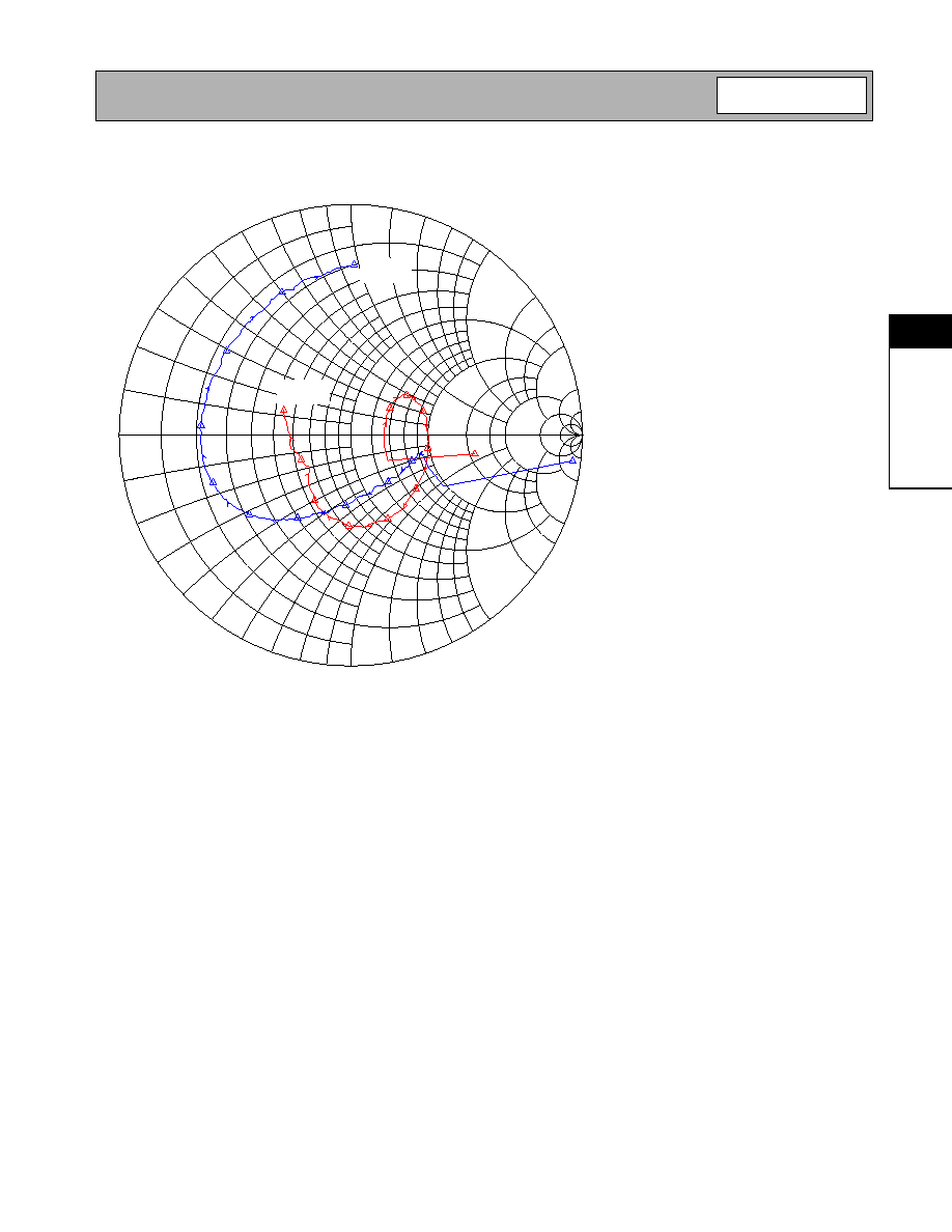
75 Ohm, 8V, 25�C
Swp Max
2.001GHz
Swp Min
0.001GHz
S[2,2]
S[1,1]

Preliminary
3-48
RF2360
Rev A9 010824
3
L
I
NE
A
R
CA
T
V
A
M
P
L
IF
IE
R
S
0
1.
0
1.
0
-1
.0
10.
0
10.0
-1
0.0
5.
0
5.0
-5
.0
2.
0
2.
0
-2
.0
3.
0
3.
0
-3
.0
4.
0
4.0
-4
.0
0.
2
0.2
-0.2
0.
4
0.
4
-0.
4
0.
6
0
.6
-0
.6
0.
8
0
.8
-0
.8
50 Ohm, 8V - Return Loss
Swp Max
3000MHz
Swp Min
0.03MHz
S[1,1]
S[2,2]
Preliminary
3-49
RF2360
Rev A9 010824
3
L
I
NE
A
R
CA
T
V
A
M
P
L
IF
IE
R
S
0
1.
0
1.
0
-1
.0
10.
0
10.0
-1
0.0
5.
0
5.0
-5
.0
2.
0
2.
0
-2
.0
3.
0
3.
0
-3
.0
4.
0
4.0
-4
.0
0.
2
0.2
-0.2
0.
4
0.
4
-0.
4
0.
6
0
.6
-0
.6
0.
8
0
.8
-0
.8
75 Ohm, 8V - Return Loss
Swp Max
3000MHz
Swp Min
1MHz
S[1,1]
S[2,2]

Preliminary
3-50
RF2360
Rev A9 010824
3
L
I
NE
A
R
CA
T
V
A
M
P
L
IF
IE
R
S